

查询HCF4022 供应商
HCF4022B
OCTAL COUNTER WIT H 8 DECODED OUTPUTS
■ MEDIUM SPEED OPERATION :
10 MHz (Typ.) at V
■ FULLY STATIC OPERATION
■ STAND ARDIZED SYMMETRICAL OUTPUT
DD
= 10V
CHARACTERISTICS
■ QUIESCENT CURRENT SPECIFIED UP TO
20V
■ 5V, 10V AND 15V PARAMETRIC RATINGS
■ INPUT LEAKAGE CURRENT
I
= 100nA (MAX) AT VDD = 18V TA = 25°C
I
■ 100% TESTED FOR QUIESCENT CURRENT
■ MEETS ALL REQUIREMENTS OF JEDEC
JESD13B " STANDARD SPECIF ICATIONS
FOR DESCRIPTI ON OF B SERI ES CMOS
DEVICES"
DESCRIPTION
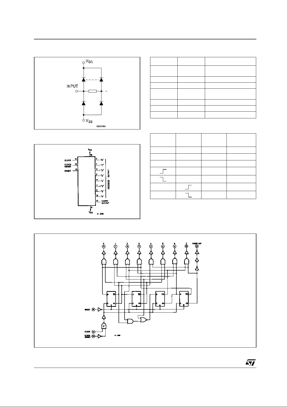
The HCF4022B is a m onolithic integrated circuit
fabricated in Metal Oxide Semiconductor
technology available in DIP and SOP packages.
The HCF4022B is 4-stage Johnson counter
having 8 decoded outputs. Inputs include a
CLOCK, a RESET, and a CLOCK INHIBIT signal.
Schmitt trigger action in the clock input circuit
provides pulse shaping that allows unlimited clock
input pulse rise and fall times. This counter is
advanced one count at the positive clock signal
transition if the CLOCK INHIBIT signal is low.
Counter advanced via the clock line is inhibited
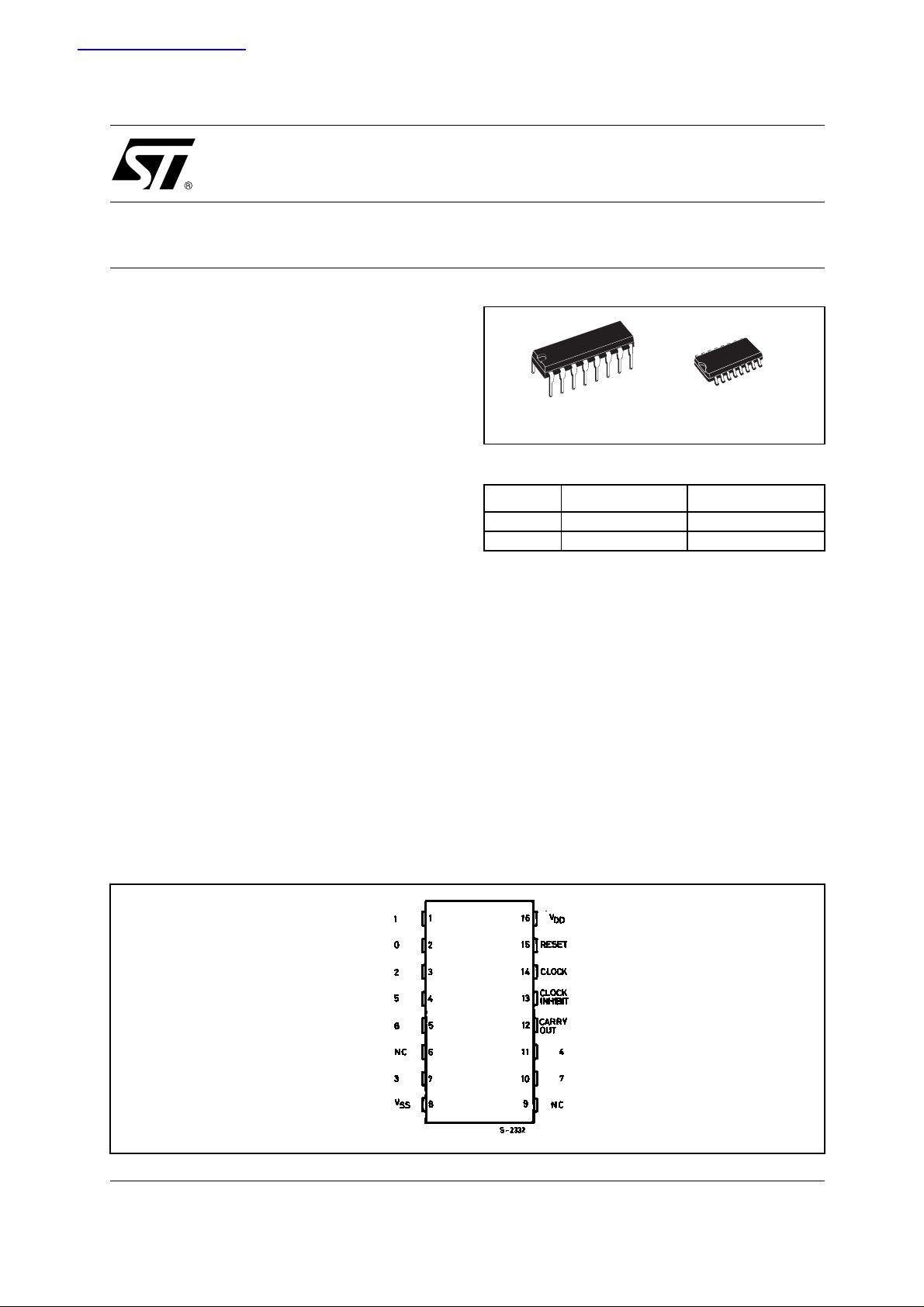
DIP SOP
ORDER CODES
PACKAGE TUBE T & R
DIP HCF4022BEY
SOP HCF4022BM1 HCF4022M013TR
when the CLOCK I NHIBIT signal is high. A high
RESET signal clears the counter to it s ze r o co unt.
Use of the Johnson decade-counter configuration
permits high speed operation, 2-input decimal
decode gating and spike-free decoded outputs.
Anti-lock gating is provided, thus assuring p roper
counting sequence. The decoded outputs are
normally low and go high only at their respective
decoded time slot. Eac h decoded ou tput remains
high for one full clock cycle. A CARRY - OUT
signal completes one cycle every 8 clock input
cycles and is used to ripple-clock the succeeding
device in a multi-device counting chain.
PIN CONNECTION
1/11September 2001
HCF4022B
INPUT EQUIVALENT CIRCUIT
FUNCTIONAL DIAGRAM
PIN DESCRIPTION
PIN No SYMBOL NAME AND FUNCTION
2, 1, 3, 7, 1 1,
4, 5, 10
0 to 7 Decoded Output
6, 9 NC Not Connected
14 CLOCK Clock Input
13
CLOCK
INHIBIT
Clock Inhibit Input
15 RESET Reset Input
12 CARRY OUT Carry Output
8
V
SS
Negative Supply Voltage
TRUTH TABLE
CLOCK
CLOCK
INHIBIT
RESET
XXH
LXL
XHL
LL
LL
HL
HL
X : Don’t Care
Qn : No Ch ange
DECODED
OUTPUT
Q
Q
Q
0
Q
n
Q
n
n+1
Q
n
Q
n
n+1
LOGIC DIAGRAM
This log i c diagram has not be used to estimat e propagation del ays
2/11
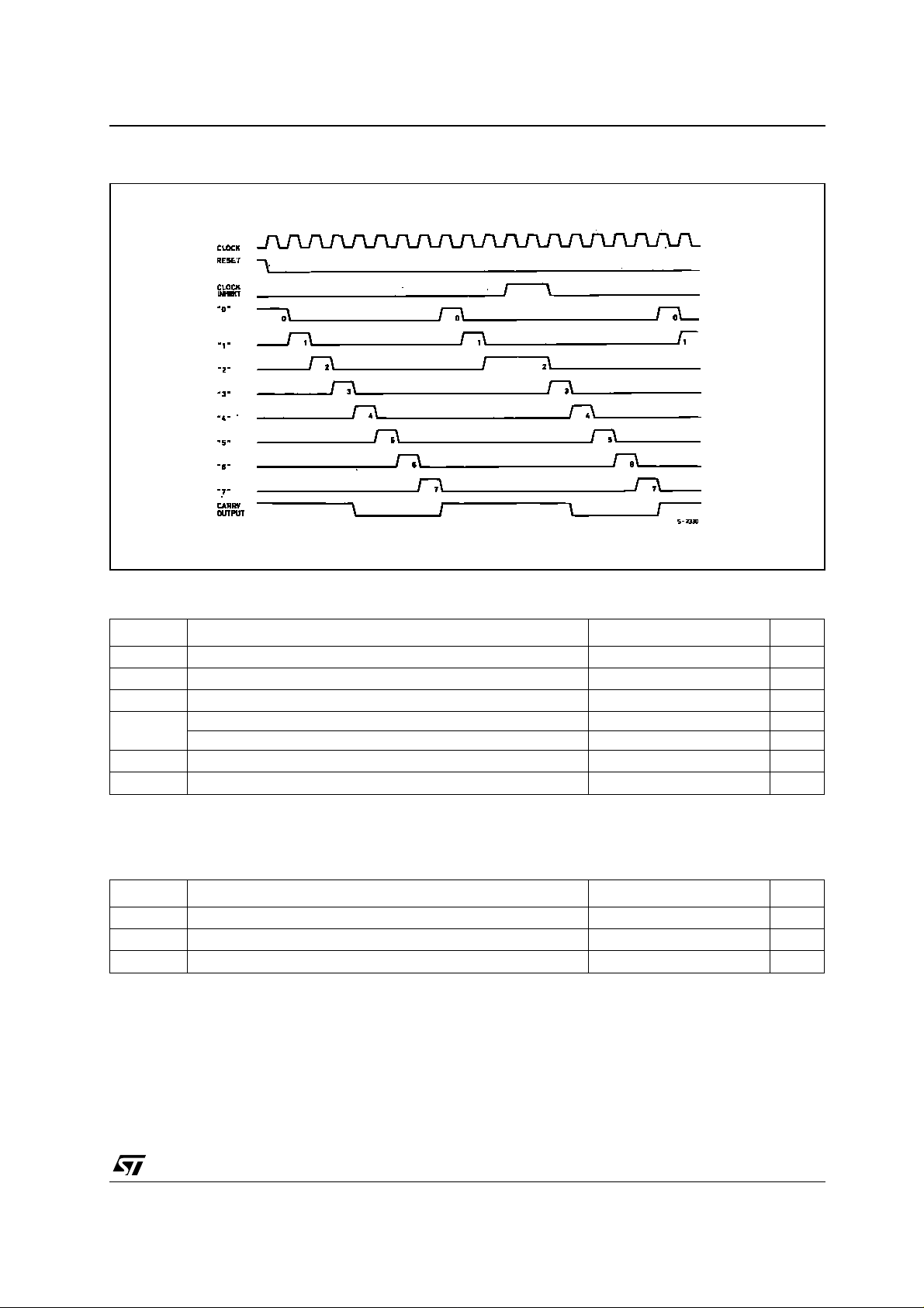
TIMING CHART
HCF4022B
ABSOLUTE MAXIMUM RATINGS
Symbol Parameter Value Unit
V
V
P
Supply Voltage
DD
DC Input Voltage -0.5 to VDD + 0.5
I
I
DC Input Current
I
Power Dissipation per Package 200 mW
D
-0.5 to +22 V
± 10 mA
V
Power Dissipation per Output Transistor 100 mW
T
T
Absolute Maximum Ratings are those values beyond which damage to the device may occur. Functional operation under these conditions is
not implied.
All voltage values ar e referred to V
Operating Temperature
op
Storage Temperature
stg
pin voltage.
SS
-55 to +125 °C
-65 to +150 °C
RECOMMENDED OPERATING CONDITIONS
Symbol Parameter Value Unit
V
V
T
Supply Voltage
DD
Input Voltage 0 to V
I
Operating Temperature
op
3 to 20 V
DD
-55 to 125 °C
V
3/11
HCF4022B
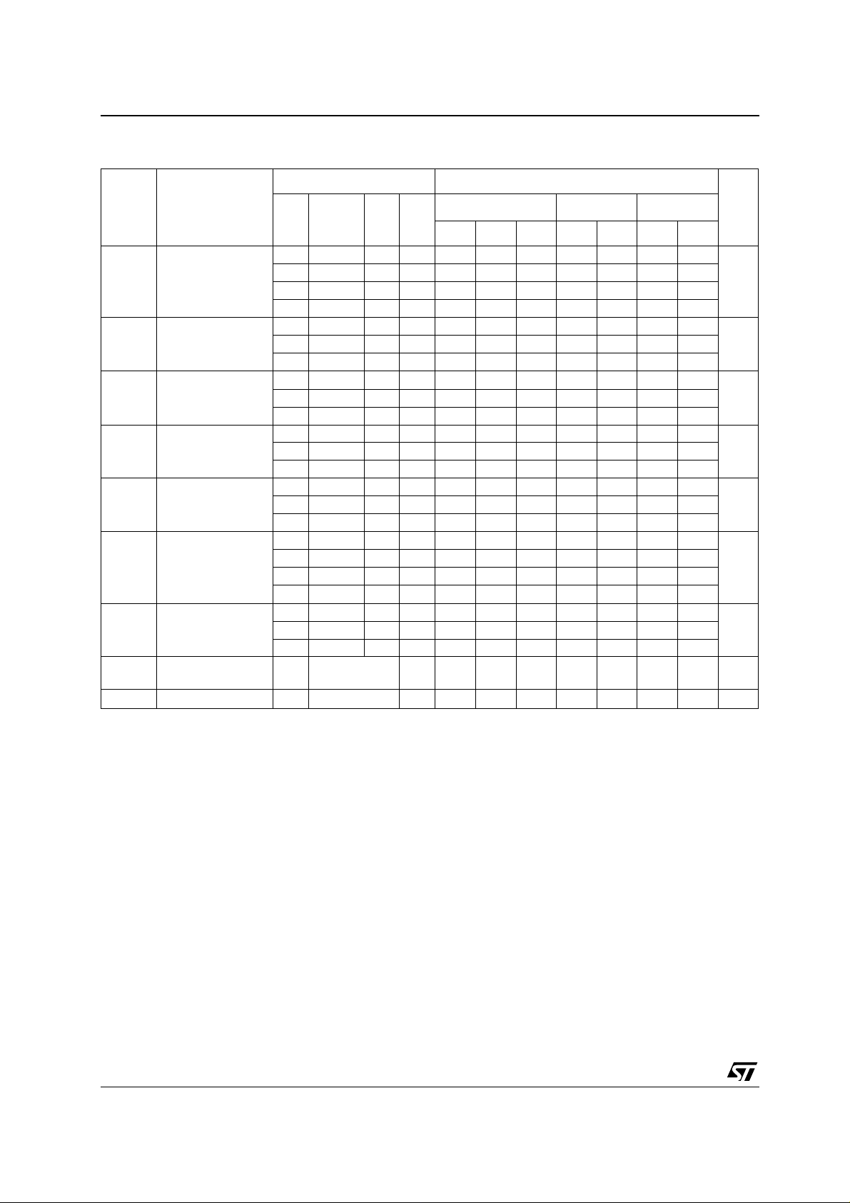
DC SPECIFICATIONS
Test Condition Value
T
Symbol Parameter
I
Quiescent Current 0/5 5 0.04 5 150 150
L
V
(V)
V
I
(V)
|I
|
O
O
(µA)
V
DD
(V)
= 25°C
A
Min. Typ. Max. Min. Max. Min. Max.
0/10 10 0.04 10 300 300
0/15 15 0.04 20 600 600
0/20 20 0.08 100 3000 3000
V
High Level Output
OH
Voltage
0/5 <1 5 4.95 4.95 4.95
0/15 <1 15 14.95 14.95 14.95
Low Level Output
V
OL
Voltage
5/0 <1 5 0.05 0.05 0.05
15/0 <1 15 0.05 0.05 0.05
High Level Input
V
IH
Voltage
0.5/4.5 <1 5 3.5 3.5 3.5
1.5/13.5 <1 15 11 11 11
V
IL
Low Level Input
Voltage
4.5/0.5 <1 5 1.5 1.5 1.5
13.5/1.5 <1 15 4 4 4
I
OH
Output Drive
Current
0/5 2.5 <1 5 -1.36 -3.2 -1.1 -1.1
0/5 4.6 <1 5 -0.44 -1 -0.36 -0.36
0/10 9.5 <1 10 -1.1 -2.6 -0.9 -0.9
0/15 13.5 <1 15 -3.0 -6.8 -2.4 -2.4
I
OL
Output Sink
Current
0/5 0.4 <1 5 0.44 1 0.36 0.36
0/15 1.5 <1 15 3.0 6.8 2.4 2.4
Input Leakage
I
I
Current
C
Input Capacitance
I
The Noi se Margin for bot h " 1" and "0" level is: 1V min. with VDD=5V, 2V min. with VDD=10V, 2.5V min. with VDD=15V
0/18 Any Input 18
Any Input 5 7.5 pF
±10
-5
-40 to 85°C -55 to 125°C
±0.1 ±1 ±1 µA
Unit
µA
V0/10 <1 10 9.95 9.95 9.95
V10/0 <1 10 0.05 0.05 0.05
V1/9 <1 10 7 7 7
V9/1 <1 10 3 3 3
mA
mA0/10 0.5 <1 10 1.1 2.6 0.9 0.9
4/11

HCF4022B
DYNAMIC ELECTRICAL CHARACTERISTICS (T
Symbol Parameter
CLOCKED OPERATION
t
PLH tPHL
Propagation Delay Time
(decode out)
Propagation Delay Time
(carry out)
t
THL tTLH
f
CL
t
t
setup
Transition Time (carry out
or decoded out lines)
(1)
Maximum Clock Input
Frequency
Minimum Clock Pulse
t
W
Width
Clock Input Rise or Fall
, t
r
f
Time
Data Setup Time Minimum
Clock Inhibit
RESET OPERATION
t
PLH, tPHL
Propagation Delay Time
(carry out or decoded out
lines)
Minimum Reset Pulse
t
W
Width
t
REM
(*) Typical temperature coefficient for all VDD value is 0.3 %/°C.
(1) Measured with re spect to carry out line.
Minimum Reset Removal
Time
(V)
V
DD
5 325 650
15 85 170
5 300 600
15 80 160
5 100 200
15 40 80
5 2.5 5 5
15 5.5 11
5 100 200
15 30 60
5
15
5 115 230
15 35 75
5 265 530
15 85 170
5 130 260
15 30 60
5 200 400
15 75 150
= 25°C, CL = 50pF, RL = 200KΩ, tr = tf = 20 ns)
amb
Test Condition Value (*) Unit
Min. Typ. Max.
ns10 135 270
ns10 125 250
ns10 50 100
MHz10 5 10
ns10 45 90
unlimited µs10
ns10 50 100
ns10 115 230
ns10 55 110
ns10 140 280
5/11

HCF4022B
TYPICAL APPLICATIONS
DIVIDE BY N COUNTER(N <
DECODED OUTPUTS
TEST CIRCUIT
10) WITH
When the N
th
decoded output is reached (N
clock pulse) the S-R flip-flop (constructed from two
NOR gates of the HCF 4001B) generates a reset
pulse which clears the HCF4022B to its zero
count. At this time, if the N
greater than or equal to 6, the C
th
decoded output is
line goes high
OUT
to clock the next HCF4022B counter section. The
"0" decoded output also goes high at this time.
Coincidence of the clock low and decoded "0"
output high resets the S-R flip-flop to enable the
HCF4022B. If the N
th
decoded output i s le ss th an
6, the COUT line will not go high and, therefore,
cannot be used. In this case "0" decoded out put
may be used to perform the clocking function for
the next counter.
th
CL = 50pF or equivalent (includes jig and probe capacitanc e)
R
= 200KΩ
L
R
= Z
of pulse generator (typically 50Ω)
T
OUT
6/11

WAVEFORM 1 : PROPAGATION DELAY TIMES (f=1MHz; 50% duty cycle)
HCF4022B
WAVEFORM 2 : MINIMUM SETUP TIME (CLOCK INHIBIT TO CLOCK) (f=1MHz; 50% duty cycle)
7/11

HCF4022B
WAVEFORM 3 : PROPAGA TION DELAY TIME S, MINIMUM RESET PULSE WIDTH (f=1MHz; 50% duty
cycle)
WAVEFORM 4 : MINIMUM SETUP TIME (CLOCK TO CLOCK INHIBIT) (f=1 MHz; 50% duty cycle)
8/11

HCF4022B
Plastic DIP-16 (0.25) MECHANICAL DATA
mm. inch
DIM.
MIN. TYP MAX. MIN. TYP. MAX.
a1 0.51 0.020
B 0.77 1.65 0.030 0.065
b 0.5 0.020
b1 0.25 0.010
D 20 0.787
E 8.5 0.335
e 2.54 0.100
e3 17.78 0.700
F 7.1 0.280
I 5.1 0.201
L 3.3 0.130
Z 1.27 0.050
P001C
9/11

HCF4022B
SO-16 MECHANICAL DATA
DIM.
A 1.75 0.068
a1 0.1 0.2 0.003 0.007
a2 1.65 0.064
b 0.35 0.46 0.013 0.018
b1 0.19 0.25 0.007 0.010
C 0.5 0.019
c1 45° (typ.)
D 9.8 10 0.385 0.393
E 5.8 6.2 0.228 0.244
e 1.27 0.050
e3 8.89 0.350
F 3.8 4.0 0.149 0.157
G 4.6 5.3 0.181 0.208
L 0.5 1.27 0.019 0.050
M 0.62 0.024
S8° (max.)
MIN. TYP MAX. MIN. TYP. MAX.
mm. inch
10/11
PO13H

HCF4022B
Information furnished is bel ieved to be accurate and reliable. However, STMicroe lectronics assumes no responsibility for the
consequences of use of such information nor for any infringement of patents or other rights of third parties which may result from
its use. No li cense is granted by implication or otherwise under any patent or patent righ ts of S TMic roelec tronics. Specifications
mentioned in this publication ar e subject to change without notice. This publication supersedes and replaces all information
previously supplied. S TMicroelectronics products are not authorized for use as critica l components in life suppo rt devices or
systems without express written approval of STMicroelectronics.
Australi a - Brazil - China - Finland - France - Germany - Hong Kong - Indi a - Italy - Japan - Malaysia - Ma l ta - Morocco
© The ST logo is a registered trademark of STMicroelectronics
© 2001 STM icroelectr o n ics - Printed in Italy - All Righ ts Reserved
STMicr o el ectronics GROU P OF COMPANIES
Singapo re - Spain - Swe den - Switzerland - United K i ngdom
© http://www.st.com
11/11
 Loading...