

HCF4017B
DECADE COUNTER WITH 10 DECODED OUTPUTS
■ MEDIUM SPEED OPERATION :
10 MHz (Typ.) at V
■ FULLY STATIC OPERATION
■ STAND ARDIZED SYMMETRICAL OUTPUT
DD
= 10V
CHARACTERISTICS
■ QUIESCENT CURRENT SPECIFIED UP TO
20V
■ 5V, 10V AND 15V PARAMETRIC RATINGS
■ INPUT LEAKAGE CURRENT
I
= 100nA (MAX) AT VDD = 18V TA = 25°C
I
■ 100% TESTED FOR QUIESCENT CURRENT
■ MEETS ALL REQUIREMENTS OF JEDEC
JESD13B " STANDARD SPECIF ICATIONS
FOR DESCRIPTI ON OF B SERI ES CMOS
DEVICES"
DESCRIPTION
The HCF4017B is a m onolithic integrated circuit
fabricated in Metal Oxide Semiconductor
technology available in DIP and SOP packages.
The HCF4017B is 5-stage Johnson counter
having 10 decoded outputs. Inputs include a
CLOCK, a RESET, and a CLOCK INHIBIT signal.
Schmitt trigger action in the clock input circuit
provides pulse shaping that allows unlimited clock
input pulse rise and fall times. This counter is
advanced one count at the positive clock signal
transition if the CLOCK INHIBIT signal is low.
Counter advanced via the clock line is inhibited
DIP SOP
ORDER CODES
PACKAGE TUBE T & R
DIP HCF4017BEY
SOP HCF4017BM1 HCF4017M013TR
when the CLOCK I NHIBIT signal is high. A high
RESET signal clears the counter to it s ze r o co unt.
Use of the Johnson decade-counter configuration
permits high speed operation, 2-input decimal
decode gating and spike-free decoded outputs.
Anti-lock gating is provided, thus assuring p roper
counting sequence. The decoded outputs are
normally low and go high only at their respective
decoded time slot. Eac h decoded ou tput remains
high for one full clock cycle. A CARRY - OUT
signal completes one cy cle every 10 clock input
cycles and is used to ripple-clock the succeeding
device in a multi-device counting chain.
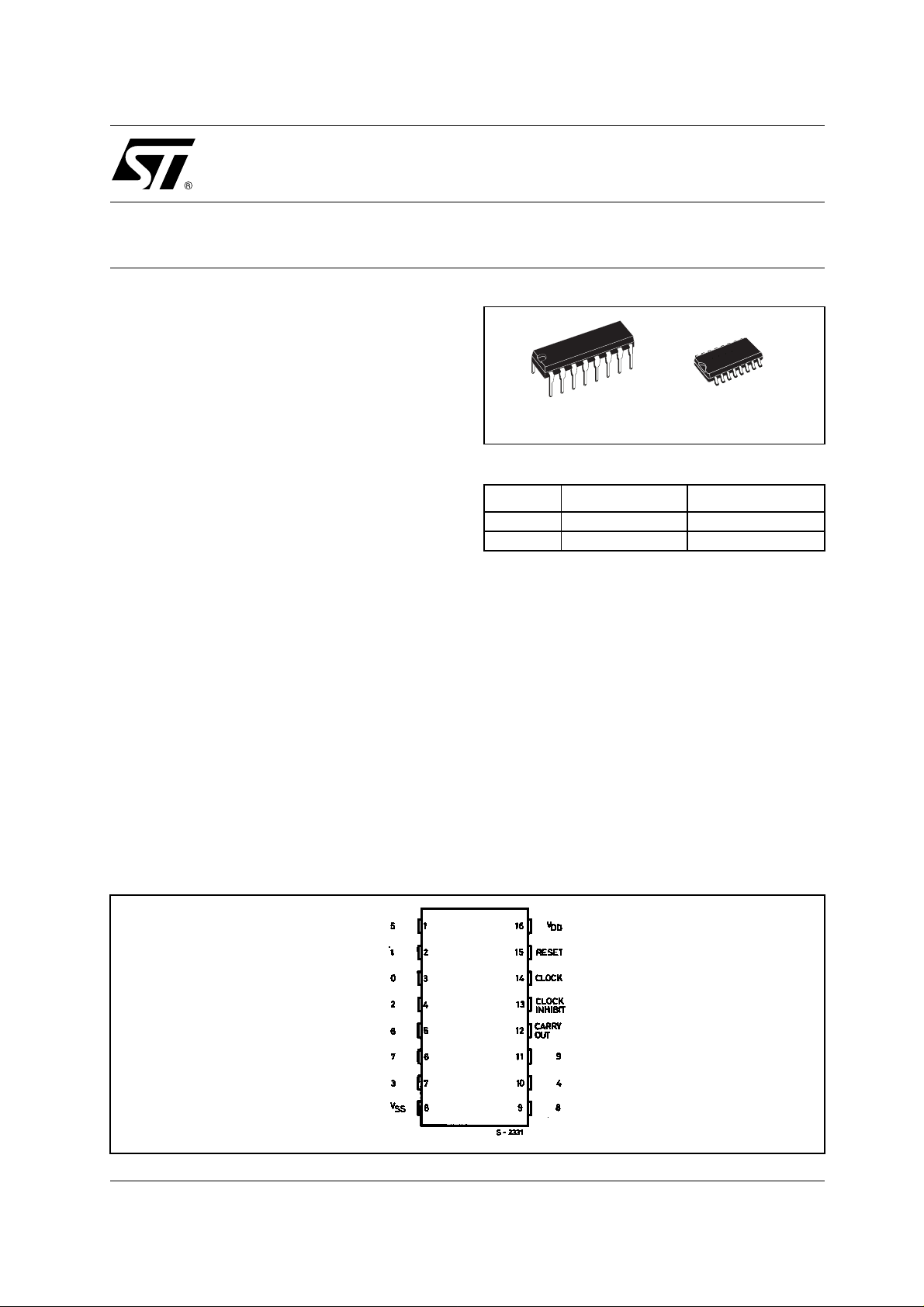
PIN CONNECTION
1/11September 2001
HCF4017B
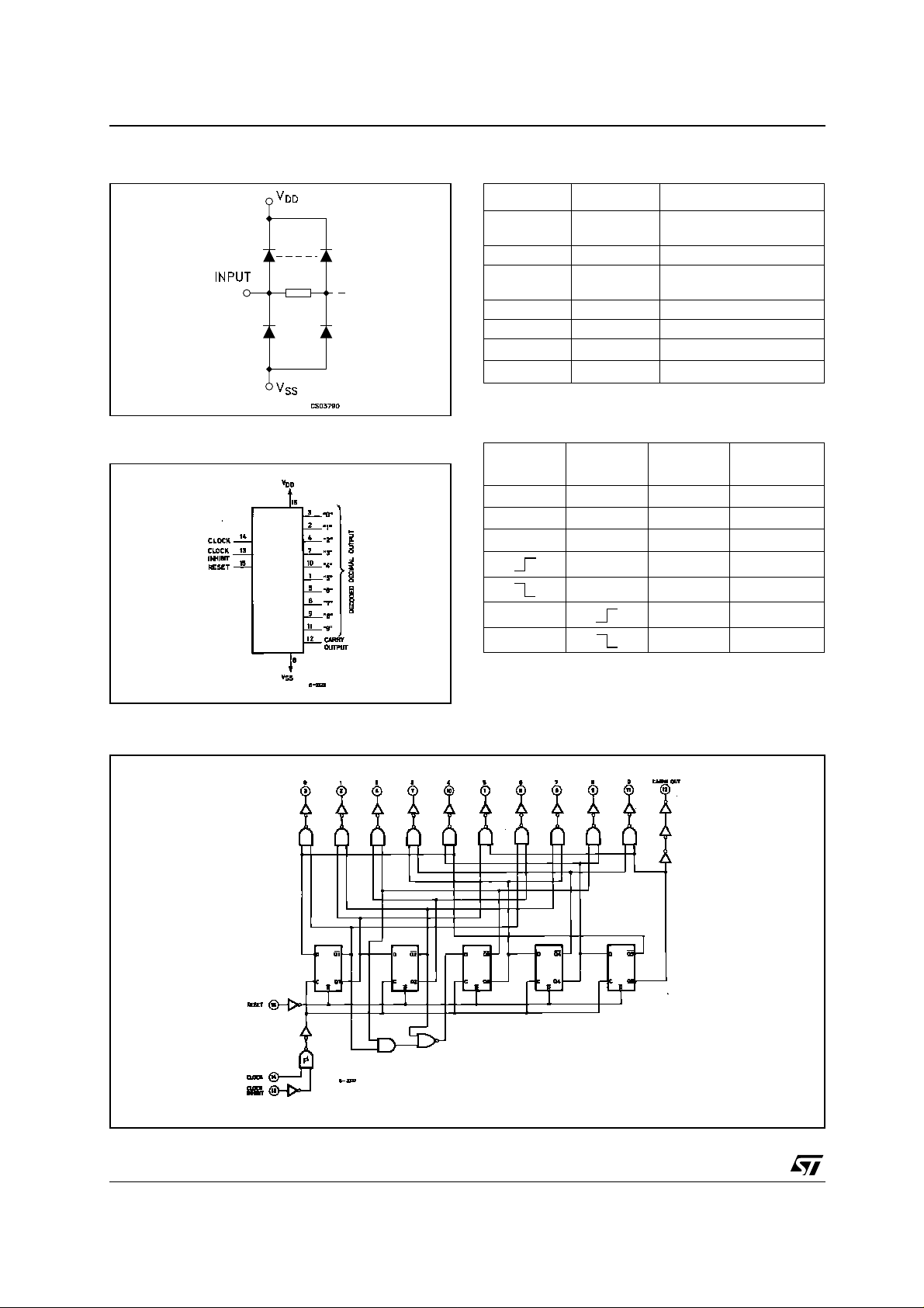
INPUT EQUIVALENT CIRCUIT
FUNCTIONAL DIAGRAM
PIN DESCRIPTION
PIN No SYMBOL NAME AND FUNCTION
3, 2, 4, 7, 10,
1, 5, 6, 9, 11
0 to 9 Decoded Decimal Output
14 CLOCK Clock Input
13
CLOCK
INHIBIT
Clock Inhibit Input
15 RESET Reset Input
12 CARRY OUT Carry Output
16
8
V
SS
V
DD
Negative Supply Voltage
Positive Supply Voltage
TRUTH TABLE
CLOCK
CLOCK
INHIBIT
RESET
XXH
LXL
XHL
LL
LL
HL
HL
DECODED
OUTPUT
Q
Q
Q
0
Q
n
Q
n
n+1
Q
n
Q
n
n+1
LOGIC DIAGRAM
X : Don’t Care
Qn : No Ch ange
This log i c diagram has not be used to estimat e propagation del ays
2/11
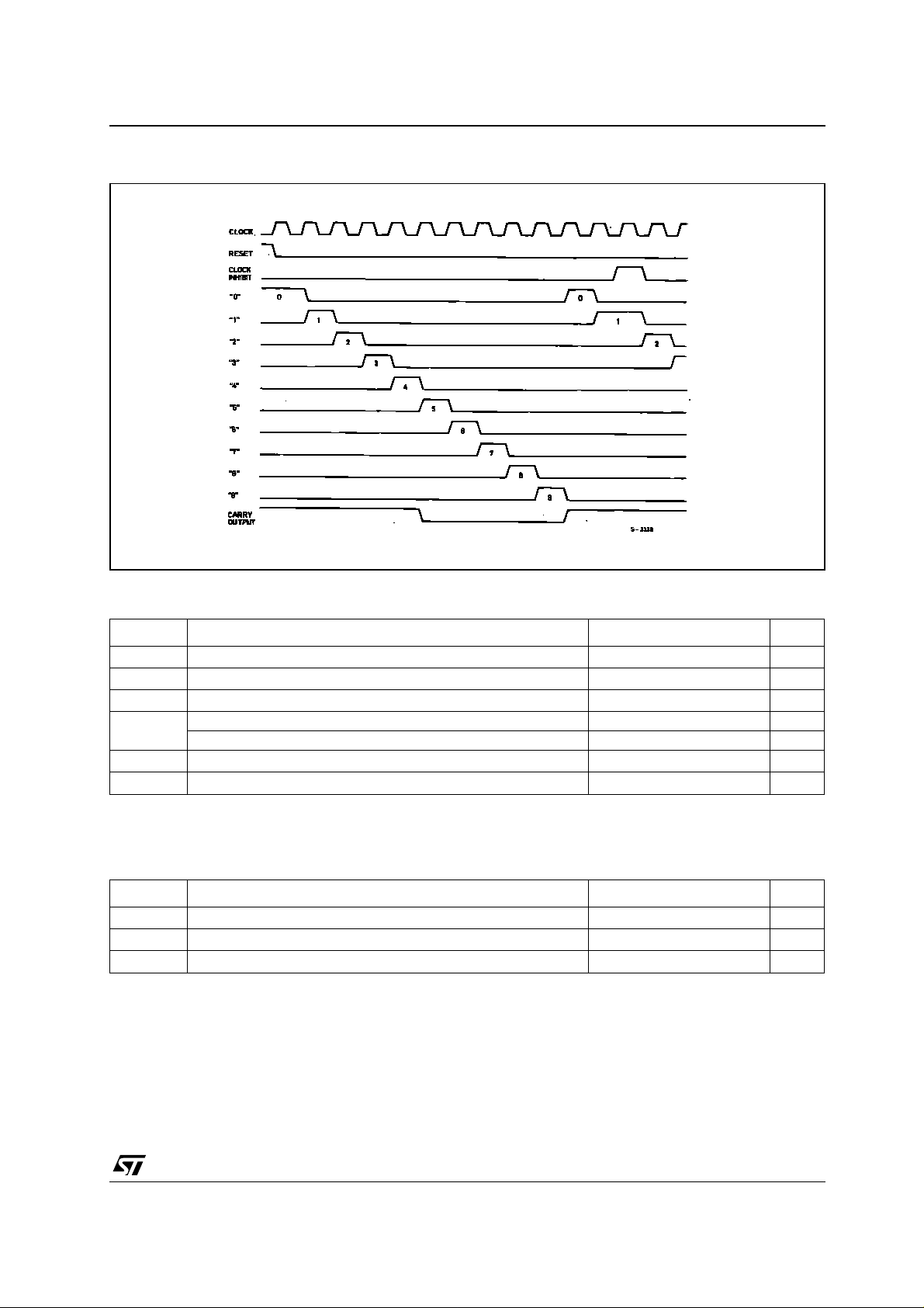
TIMING CHART
HCF4017B
ABSOLUTE MAXIMUM RATINGS
Symbol Parameter Value Unit
V
V
P
Supply Voltage
DD
DC Input Voltage -0.5 to VDD + 0.5
I
I
DC Input Current
I
Power Dissipation per Package 200 mW
D
-0.5 to +22 V
± 10 mA
V
Power Dissipation per Output Transistor 100 mW
T
T
Absolute Maximum Ratings are those values beyond which damage to the device may occur. Functional operation under these conditions is
not implied.
All voltage values ar e referred to V
Operating Temperature
op
Storage Temperature
stg
pin voltage.
SS
-55 to +125 °C
-65 to +150 °C
RECOMMENDED OPERATING CONDITIONS
Symbol Parameter Value Unit
V
V
T
Supply Voltage
DD
Input Voltage 0 to V
I
Operating Temperature
op
3 to 20 V
DD
-55 to 125 °C
V
3/11
HCF4017B
DC SPECIFICATIONS
Test Condition Value
T
Symbol Parameter
I
Quiescent Current 0/5 5 0.04 5 150 150
L
V
(V)
V
I
(V)
|I
|
O
O
(µA)
V
DD
(V)
= 25°C
A
Min. Typ. Max. Min. Max. Min. Max.
0/10 10 0.04 10 300 300
0/15 15 0.04 20 600 600
0/20 20 0.08 100 3000 3000
V
High Level Output
OH
Voltage
0/5 <1 5 4.95 4.95 4.95
0/15 <1 15 14.95 14.95 14.95
Low Level Output
V
OL
Voltage
5/0 <1 5 0.05 0.05 0.05
15/0 <1 15 0.05 0.05 0.05
High Level Input
V
IH
Voltage
0.5/4.5 <1 5 3.5 3.5 3.5
1.5/13.5 <1 15 11 11 11
V
IL
Low Level Input
Voltage
4.5/0.5 <1 5 1.5 1.5 1.5
13.5/1.5 <1 15 4 4 4
I
OH
Output Drive
Current
0/5 2.5 <1 5 -1.36 -3.2 -1.1 -1.1
0/5 4.6 <1 5 -0.44 -1 -0.36 -0.36
0/10 9.5 <1 10 -1.1 -2.6 -0.9 -0.9
0/15 13.5 <1 15 -3.0 -6.8 -2.4 -2.4
I
OL
Output Sink
Current
0/5 0.4 <1 5 0.44 1 0.36 0.36
0/15 1.5 <1 15 3.0 6.8 2.4 2.4
Input Leakage
I
I
Current
C
Input Capacitance
I
The Noi se Margin for bot h " 1" and "0" level is: 1V min. with VDD=5V, 2V min. with VDD=10V, 2.5V min. with VDD=15V
0/18 Any Input 18
Any Input 5 7.5 pF
±10
-5
-40 to 85°C -55 to 125°C
±0.1 ±1 ±1 µA
Unit
µA
V0/10 <1 10 9.95 9.95 9.95
V10/0 <1 10 0.05 0.05 0.05
V1/9 <1 10 7 7 7
V9/1 <1 10 3 3 3
mA
mA0/10 0.5 <1 10 1.1 2.6 0.9 0.9
4/11
 Loading...