

HCF4011B
QUAD 2 INPUT NAND GATE
■ PROPAGATION DELAY TIME
t
= 60ns (Typ.) at VDD = 10V
PD
■ BUFFERED INPUTS AND OUTPUTS
■ STANDARDIZED SYMMETRICAL OUTPUT
CHARACTERISTICS
■ QUIESCENT CURRENT SPECIFIED UP TO
20V
■ 5V, 10V AND 15V PARAMETRIC RATINGS
■ INPUT LEAKAGE CURRENT
I
= 100nA (MAX) AT VDD = 18V TA = 25°C
I
■ 100% TESTED FOR QUIESCENT CURRENT
■ MEETS ALL REQUIREMENTS OF JEDEC
JESD13B " STANDARD SPECIFICATIONS
FOR DESCRIPTI ON OF B SERI ES CMOS
DEVICES"
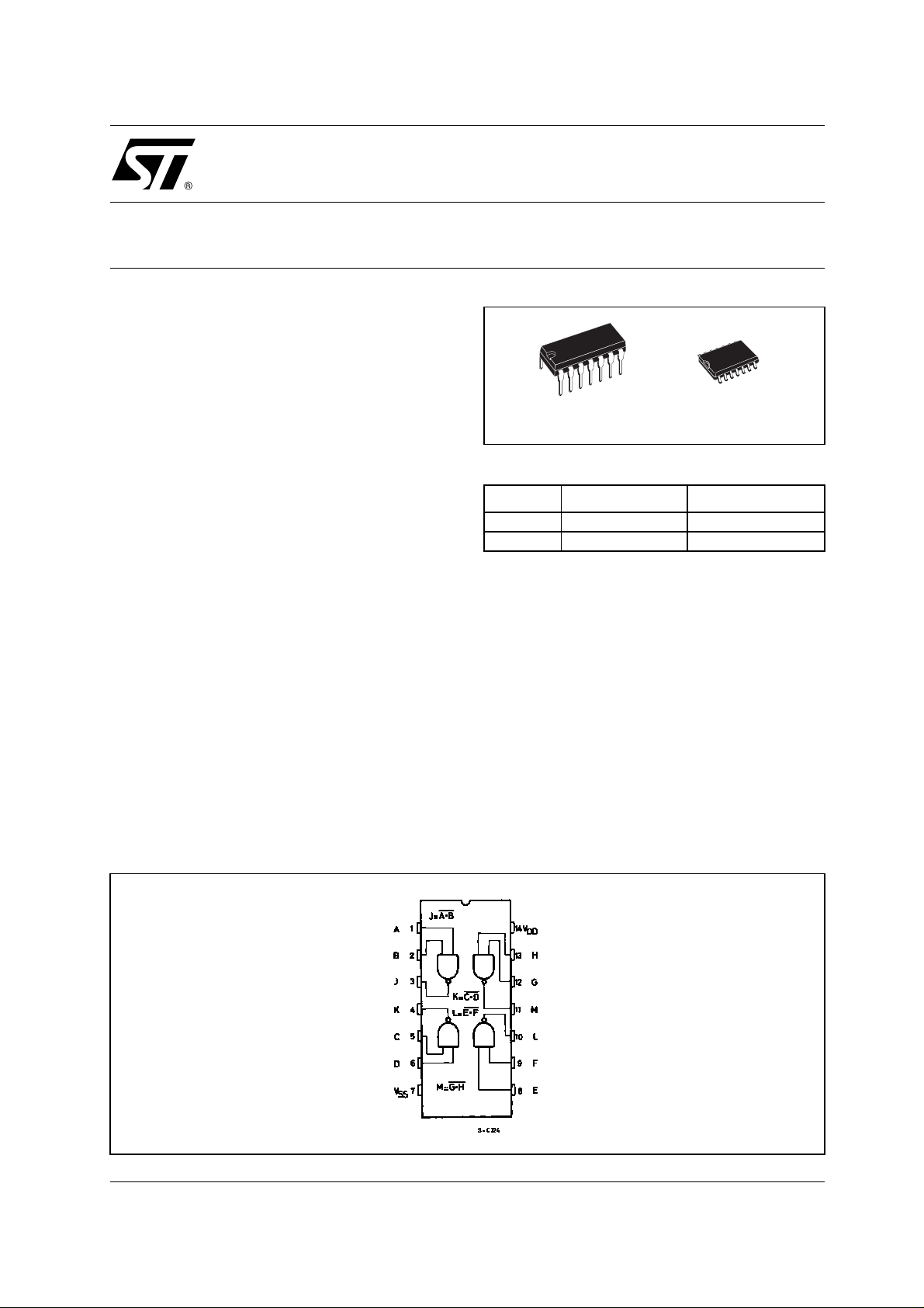
DESCRIPTION
The HCF4011B is a m onolithic integrated circuit
fabricated in Metal Oxide Semiconductor
technology available in DIP and SOP packages.
The HCF4011B QUAD 2 INPUT NAND GATE
provides the system designer with direct
DIP SOP
ORDER CODES
PACKAGE TUBE T & R
DIP HCF4011BEY
SOP HCF4011BM1 HCF4011M013TR
implementation of the NAND function and
supplement the existing family of CMOS gates. All
inputs and outputs are buffered.
PIN CONNECTION
1/7September 2001
HCF4011B
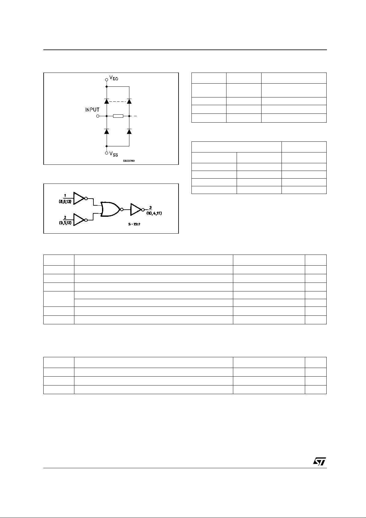
INPUT EQUIVALENT CIRCUIT
LOGIC DIAGRAM
PIN DESCRIPTION
PIN No SYMBOL NAME AND FUNCTION
1, 2, 5, 6, 8,
9, 12, 13
A, B, C, D, E,
F, G, H
Data Inputs
3, 4, 10, 11 J, K, L, M Data Outputs
14
7
V
SS
V
DD
Negative Supply Voltage
Positive Supply Voltage
TRUTH TABLE
INPUTS OUTPUTS
A, C, E, G B, D, F, H J, K, L, M
LLH
LHH
HLH
HHL
ABSOLUTE MAXIMUM RATINGS
Symbol Parameter Value Unit
V
V
P
Supply Voltage
DD
DC Input Voltage -0.5 to VDD + 0.5
I
I
DC Input Current
I
Power Dissipation per Package 200 mW
D
-0.5 to +22 V
± 10 mA
V
Power Dissipation per Output Transistor 100 mW
T
T
Absolute Maximum Ratings are those values beyond which damage to the device may occur. Functional operation under these conditions is
not implied.
All voltage values ar e referred to V
Operating Temperature
op
Storage Temperature
stg
pin voltage.
SS
-55 to +125 °C
-65 to +150 °C
RECOMMENDED OPERATING CONDITIONS
Symbol Parameter Value Unit
V
V
T
Supply Voltage
DD
Input Voltage 0 to V
I
Operating Temperature
op
3 to 20 V
DD
-55 to 125 °C
V
2/7
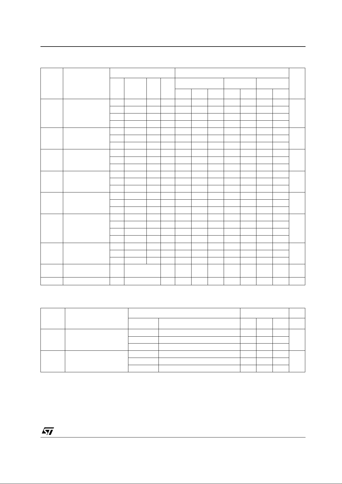
DC SPECIFICATIONS
Test Condition Value
T
Symbol Parameter
I
Quiescent Current 0/5 5 0.01 0.25 7.5 7.5
L
V
(V)
V
I
(V)
|I
|
O
O
(µA)
V
DD
(V)
= 25°C
A
Min. Typ. Max. Min. Max. Min. Max.
0/10 10 0.01 0.5 15 15
0/15 15 0.01 1 30 30
0/20 20 0.02 5 150 150
V
High Level Output
OH
Voltage
0/5 <1 5 4.95 4.95 4.95
0/15 <1 15 14.95 14.95 14.95
Low Level Output
V
OL
Voltage
5/0 <1 5 0.05 0.05 0.05
15/0 <1 15 0.05 0.05 0.05
High Level Input
V
IH
Voltage
0.5/4.5 <1 5 3.5 3.5 3.5
1.5/13.5 <1 15 11 11 11
V
IL
Low Level Input
Voltage
4.5/0.5 <1 5 1.5 1.5 1.5
13.5/1.5 <1 15 4 4 4
I
OH
Output Drive
Current
0/5 2.5 <1 5 -1.36 -3.2 -1.15 -1.1
0/5 4.6 <1 5 -0.44 -1 -0.36 -0.36
0/10 9.5 <1 10 -1.1 -2.6 -0.9 -0.9
0/15 13.5 <1 15 -3.0 -6.8 -2.4 -2.4
I
OL
Output Sink
Current
0/5 0.4 <1 5 0.44 1 0.36 0.36
0/15 1.5 <1 15 3.0 6.8 2.4 2.4
Input Leakage
I
I
Current
C
Input Capacitance
I
The Noi se Margin for both "1" and "0 " level is: 1V min. wi th VDD=5V, 2V min. with VDD=10V, 2.5V min. with VDD=15V
0/18 Any Input 18
Any Input 5 7.5 pF
±10
-5
-40 to 85°C -55 to 125°C
±0.1 ±1 ±1 µA
HCF4011B
Unit
µA
V0/10 <1 10 9.95 9.95 9.95
V10/0 <1 10 0.05 0.05 0.05
V1/9 <1 10 7 7 7
V9/1 <1 10 3 3 3
mA
mA0/10 0.5 <1 10 1.1 2.6 0.9 0.9
DYNAMIC ELECTRICAL CHARACTERISTICS (T
Symbol Param eter
t
PLH tPHL
t
TLH tTHL
(*) Typical temperat ure coefficient for all VDD value is 0.3 %/°C.
Propagation Delay Time 5 125 250
Output Transition Time 5 100 200
(V)
V
DD
15 45 90
15 40 80
= 25°C, CL = 50pF, RL = 200KΩ, tr = tf = 20 ns)
amb
Test Condition Value (*) Unit
Min. Typ. Max.
ns10 60 120
ns10 50 100
3/7
 Loading...