

■ SCHMITT TRIGGER ACTION WITH NO
EXTERNAL COMPONENTS
■ HYSTERESIS VOLTAGE (Typ.):
0.9V at V
2.3V at V
3.5V at V
■ NOISE IMMUNITY GREAT ER THAN 50%
■ NO LIMIT ON INPUT RISE AND FALL TIME
■ LOW V
=5V
DD
=10V
DD
=15V
DD
TO VSSCURRENT DURING
DD
SLOW INPUT RAMP
■ STANDARDIZED SYMMETRICAL OUTPUT
CHARACTERISTICS
■ QUIESCENT CURRE NT SPECIFIED UP TO
20V
■ 5V,10V AND 15V PARAMETRIC RATINGS
■ INPUT LEA KAGE CURRENT
I
= 100nA (MAX) AT VDD=18VTA= 25°C
I
■ 100% TESTED FOR QUIESCENT CURRENT
DESCRIPTION
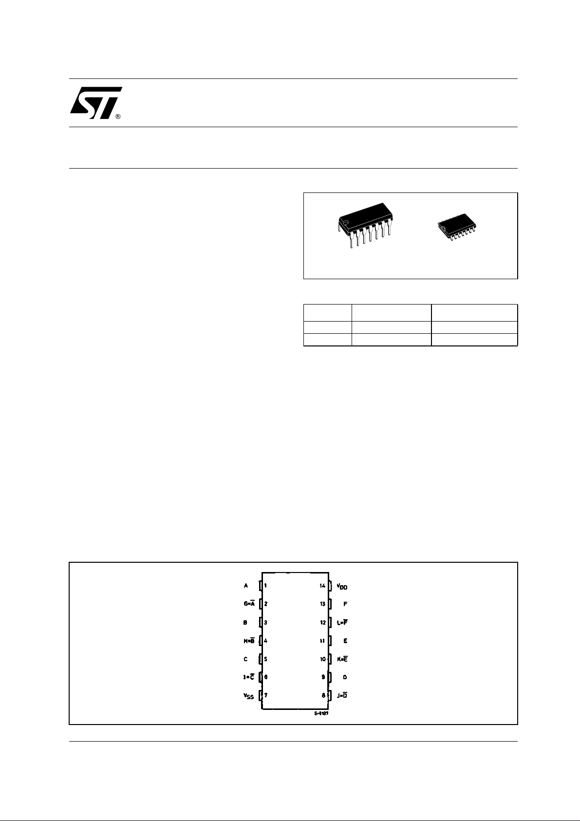
The H CF40106B is a monolithic integrated circuit
fabricated in Metal Oxide Semiconductor
technology available in DIP and SOP packages.
HCF40106B
HEX SCHMITT TRIGGER
DIP SOP
ORDER CODES
PACKAGE TUBE T & R
DIP HCF40106BEY
SOP HCF40106BM1 HCF40106M013TR
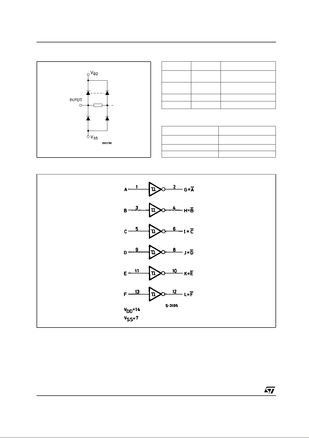
The HCF40106B consist of six Schmitt trigger
circuits. Each circuit functions as an inverter with
Schmitt trigger action on the input. The trigger
switches at different points for positive and
negative going signals. The difference between
the positive going voltage (V
going voltage (V
(V
).
H
) is defined as hysteresis voltage
N
) and the negative
P
PIN CONNE CTION
1/10March 2004
HCF40106B
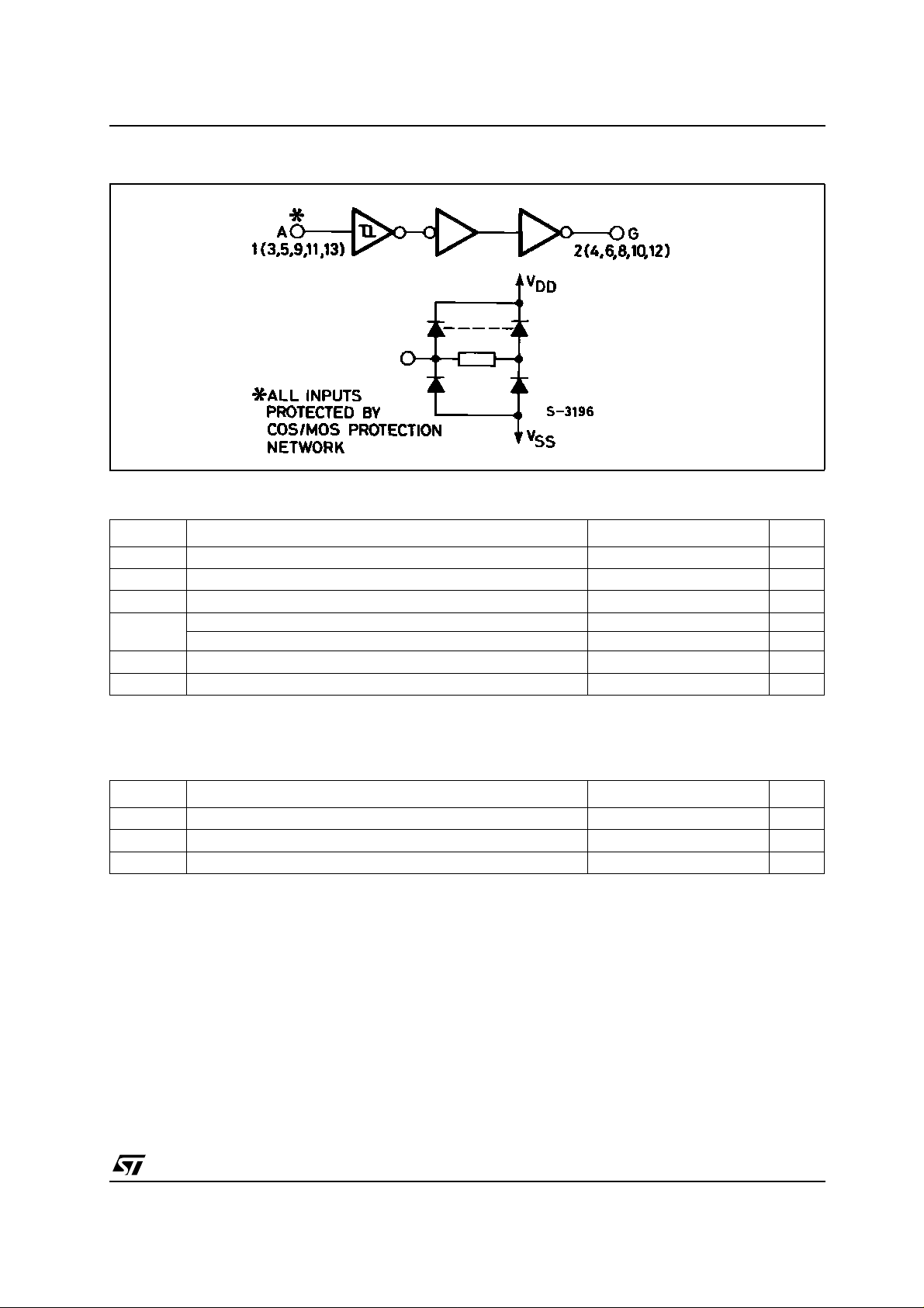
INPUT EQUIVALENT CIRCUIT PIN DESCRIPTION
PIN N° SYMBOL NAME AND FUNCTION
1, 3, 5, 9, 11,13A, B,C,D,E,
2, 4, 6, 8,10,12G, H, I, J, K,
7
14
TRUTH TABLE
INPUTS OUTPUTS
AtoF GtoL
FUNCTIONAL DIAGRAM
V
V
LH
HL
F
L
SS
DD
Data Inputs
Data Outputs
Negative Supply Voltage
Positive Supply Voltage
2/10
HCF40106B
LOGIC DIAGRAM
ABSOLUTE MAXIMUM RATING S
Symbol Parameter Value Unit
V
V
P
T
T
stg
Absolute Maximum Ratings are those values beyond which damage to the device may occur. Functional operation under these conditions is
not implied.
All voltage valuesare referred to V
Supply Voltage
DD
DC Input Voltage -0.5 to VDD+0.5
I
I
DC Input Current
I
Power Dissipation per Package 200 mW
D
-0.5 to +22 V
± 10 mA
Power Dissipation per Output Transistor 100 mW
Operating Temperature
op
Storage Temperature
pin voltage.
SS
-55 to +125 °C
-65 to +150 °C
V
RECOMMENDED OPERATING CONDITIONS
Symbol Parameter Value Unit
V
V
T
Supply Voltage
DD
Input Voltage 0 to V
I
Operating Temperature
op
3to20 V
DD
-55 to 125 °C
V
3/10

HCF40106B
DC SPECIFICATIONS
Test Condition Value
T
Symbol Parameter
I
Quiescent Current 0/5 5 0.02 1 30 30
L
V
(V)
V
|I
|
I
O
(V)
O
(µA)
V
DD
(V)
= 25°C
A
Min. Typ. Max. Min. Max. Min. Max.
0/10 10 0.02 2 60 60
0/15 15 0.02 4 120 120
0/20 20 0.04 20 600 600
V
High Level Output
OH
Voltage
0/5 <1 5 4.95 4.95 4.95
0/15 <1 15 14.95 14.95 14.95
V
Low Level Output
OL
Voltage
5/0 <1 5 0.05 0.05 0.05
15/0 <1 15 0.05 0.05 0.05
V
Positive Trigger
P
Threshold Voltage
5 2.2 2.9 3.6 2.2 3.6 2.2 3.6
15 6.8 8.8 10.8 6.8 10.8 6.8 10.8
V
Negative Trigger
N
Threshold Voltage
5 0.9 1.9 2.8 0.9 2.8 0.9 2.8
15 4 5.8 7.4 4 7.4 4 7.4
V
Hysteresis Voltage 5 0.3 0.9 1.6 0.3 1.6 0.3 1.6
H
151.63.551.651.65
I
OH
Output Drive
Current
0/5 2.5 5 -1.36 -3.2 -1.15 -1.1
0/5 4.6 5 -0.44 -1 -0.36 -0.36
0/10 9.5 10 -1.1 -2.6 -0.9 -0.9
0/15 13.5 15 -3.0 -6.8 -2.4 -2.4
I
OL
Output Sink
Current
0/5 0.4 5 0.44 1 0.36 0.36
0/15 1.5 15 3.0 6.8 2.4 2.4
I
Input Leakage
I
Current
Input Capacitance
C
I
The NoiseMargin for both "1" and "0" levelis: 1V min. with VDD=5V, 2V min. with VDD=10V, 2.5V min. with VDD=15V
0/18 Any Input 18
Any Input 5 7.5 pF
±10
-5
-40 to 85°C -55 to 125°C
±0.1 ±1 ±1 µA
Unit
µA
V0/10 <1 10 9.95 9.95 9.95
V10/0 <1 10 0.05 0.05 0.05
V10 4.6 5.9 7.1 4.6 7.1 4.6 7.1
V10 2.5 3.9 5.2 2.5 5.2 2.5 5.2
V10 1.2 2.3 3.4 1.2 3.4 1.2 3.4
mA
mA0/10 0.5 10 1.1 2.6 0.9 0.9
DYNAMIC EL ECTRICAL CHARACTERISTICS (T
Symbol Parameter
t
PLHtPHL
t
TLHtTHL
(*) Typical temperature coefficient for all VDDvalue is 0.3%/°C.
PropagationDelayTime 5 140 280
Output Transition Time 5 100 200
4/10
V
(V)
DD
15 60 120
15 40 80
= 25° C, CL= 50pF, RL= 200KΩ,tr=tf=20ns)
amb
Test Condition Value (*) Unit
Min. Typ. Max.
ns10 70 140
ns10 50 100

TYPICAL APP LICATIONS
ASTABLE MULTIVIBRATOR MONOSTABLE MULTIVIBRATOR
WAVE SHAPER
HCF40106B
5/10

HCF40106B
TEST CIRCUIT
CL= 50pF or equivalent (includes jig and probe capacitance)
=200KΩ
R
L
R
T=ZOUT
WAVEFORM: PROPAGATION DELAY TIMES (f=1MHz; 50% duty cycle)
of pulse generator (typically 50Ω)
6/10

HCF40106B
Plastic DIP-14 MECHANICAL DATA
mm. inch
DIM.
MIN. TYP MAX. MIN. TYP. MAX.
a1 0.51 0.020
B 1.39 1.65 0.055 0.065
b 0.5 0.020
b1 0.25 0.010
D 20 0.787
E 8.5 0.335
e 2.54 0.100
e3 15.24 0.600
F 7.1 0.280
I 5.1 0.201
L 3.3 0.130
Z 1.27 2.54 0.050 0.100
P001A
7/10
HCF40106B
SO-14 MECHANICAL DATA
DIM.
A 1.75 0.068
a1 0.1 0.2 0.003 0.007
a2 1.65 0.064
b 0.35 0.46 0.013 0.018
b1 0.19 0.25 0.007 0.010
C 0.5 0.019
c1 45˚ (typ.)
D 8.55 8.75 0.336 0.344
E 5.8 6.2 0.228 0.244
e 1.27 0.050
e3 7.62 0.300
F 3.8 4.0 0.149 0.157
G 4.6 5.3 0.181 0.208
L 0.5 1.27 0.019 0.050
M 0.68 0.026
S˚ (max.)
MIN. TYP MAX. MIN. TYP. MAX.
mm. inch
8
8/10
PO13G
HCF40106B
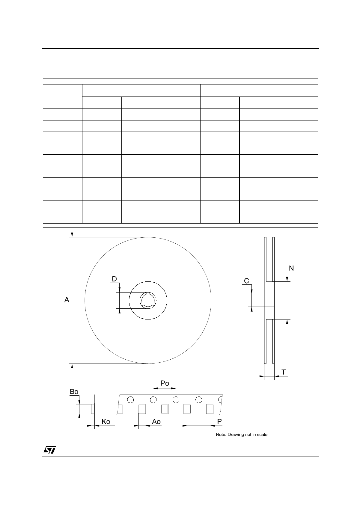
Tape & Reel SO-14 MECHANICAL DATA
mm. inch
DIM.
MIN. TYP MAX. MIN. TYP. MAX.
A 330 12.992
C 12.8 13.2 0.504 0.519
D 20.2 0.795
N 60 2.362
T 22.4 0.882
Ao 6.4 6.6 0.252 0.260
Bo 9 9.2 0.354 0.362
Ko 2.1 2.3 0.082 0.090
Po 3.9 4.1 0.153 0.161
P 7.9 8.1 0.311 0.319
9/10

HCF40106B
Information furnished is believed to be accurate and reliable. However, STMicroelectro nics assumes no responsibility for the
consequences of use of such inform ation nor fo r an y infring ement of p atents or o ther rights of third p arties which may r esult f rom
its use. No license is granted by implication or otherwise under any patent or patent rights of STMicroelectronics. Specifications
mentioned in this publication are subject to change without notice. This publication supersedes and replaces all information
previously supplied. STMicroelectronics products are not authorized for use as critical components in life support devices or
systems without express written approval of STMicroelectronics.
Australia - Belgium - B razil - Canada - China - Czech Republic - Finland - France - Germany - Hong Kong - India - Israel - Italy - Japan -
Malaysia - Malta - Morocco - Singapore - Spain - Sweden - Switzerland - United Kingdom - United States.
The ST logo is a registered trademark of STMicroelectronics
All other names are the property of their r espective owners
© 2004 STMicroelectronics - All Rights Reserved
STMicroelectronics GROUP OF COMPANIES
http://www.st.com
10/10
 Loading...