

HCF40103B
8-STAGE PRESETTABLE SYNCHRONOUS
8 BIT BINARY DOWN COUNTERS
■ SYNCHRONOUS OR ASYNCHRONOUS
PRESET
■ MEDIUM -SPEED OPERATION :
f
=3.6MHz (Typ.) at VDD = 10V
CL
■ CASCADABLE
■ QUIESCENT CURRENT SPECIF . UP TO 20V
■ 5V , 10V AND 15V P ARAMETRIC RATINGS
■ INPUT LEAKAGE CURRENT
= 100nA (MAX) AT VDD = 18V TA = 25°C
I
I
■
100% TESTED FOR QUIESCENT CURRENT
■ MEETS ALL REQUIREMENTS OF JEDEC
JESD13B "STANDARD SPECIFICATIONS
FOR DESCRIPTI ON OF B SERI ES CMOS
DEVICES"
DESCRIPTION
HCF40103B is a monolithic integrated circuit
fabricated in Metal Oxide Semiconductor
technology available in DIP and SOP packages.
HCF40103B consists of an 8-stag e synchronous
down counter with a single output that is active
when the internal count is zero. This device
contains a single 8-bit binary counter. It has
control inputs for enabling or disabling the clock,
for clearing the counter to its maximum count, and
for presetting the count er either synchronou sly or
asynchronously. All control inputs and the
CARRY-OUT/ZERO DETECT
output are
active-low logics. In normal operation, the counter
is decremented by one count on each positive
transition of the CLOCK. Counting is inhibited
when the CARRY-IN/COUNTER ENABLE
(CI/
DIP SOP
ORDER CODES
PACKAGE TUBE T & R
DIP HCF40103BEY
SOP HCF40103BM1 HCF40103M013TR
CE) input is high. The CARRY-OUT/ZERO
DETECT (CO/ZD) output goes low when the
count reaches zero if the CI/CE
input is low, and
remains low for one full clock period. When the
SYNCHRONOUS PRESET ENABLE
(SPE ) input
is low, data at the JAM input is clocked into the
counter on the next positive clock transition
regardless of the state of the CI
the ASYNCHRONOUS PRESET ENABLE
/CE input. When
(APE )
input is low, data at the JAM inputs is
asynchronously forced into the counter regardless
of the state of the S PE
, CI/CE, or CLOCK inputs.
JAM inputs J0-J7 represent a single 8 bit binary
word. When the CLEAR (CLR
) input is low, the
counter is asynchronously cleared to its maximum
count (255
) regardless of the state of any other
10
input. The precedent relation sh ip between c ontro l
input is indicated in the truth table. If all control
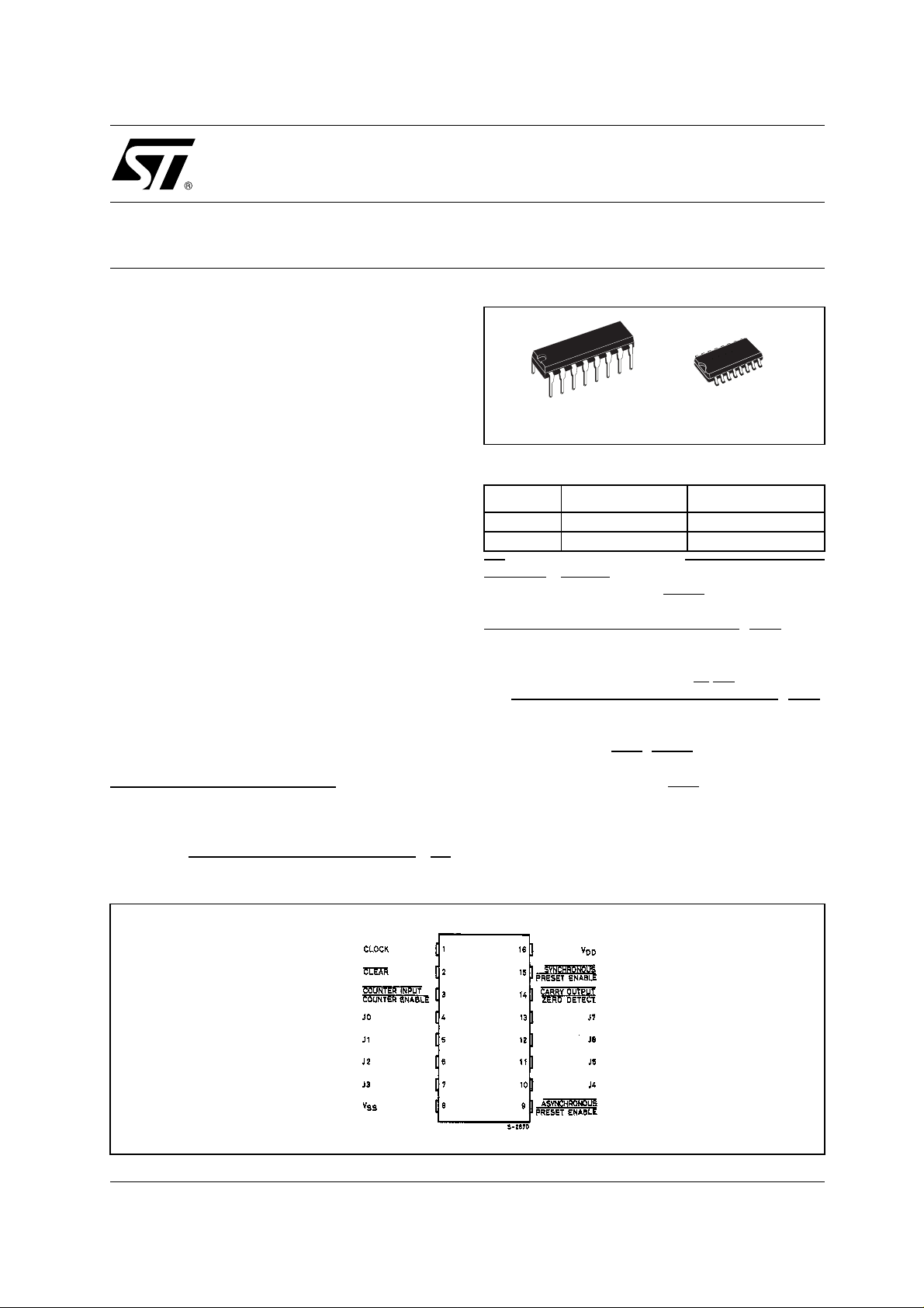
PIN CONNECTION
1/14September 2002
HCF40103B
inputs are high at the time of zero count, the
counters will jump to the maximum count, giving a
counting sequence of 256 clock pulses long.
HCF40103B m ay be cascaded using the CI/CE
input and the CO/ZD output, in either a
synchronous or ripple mode.
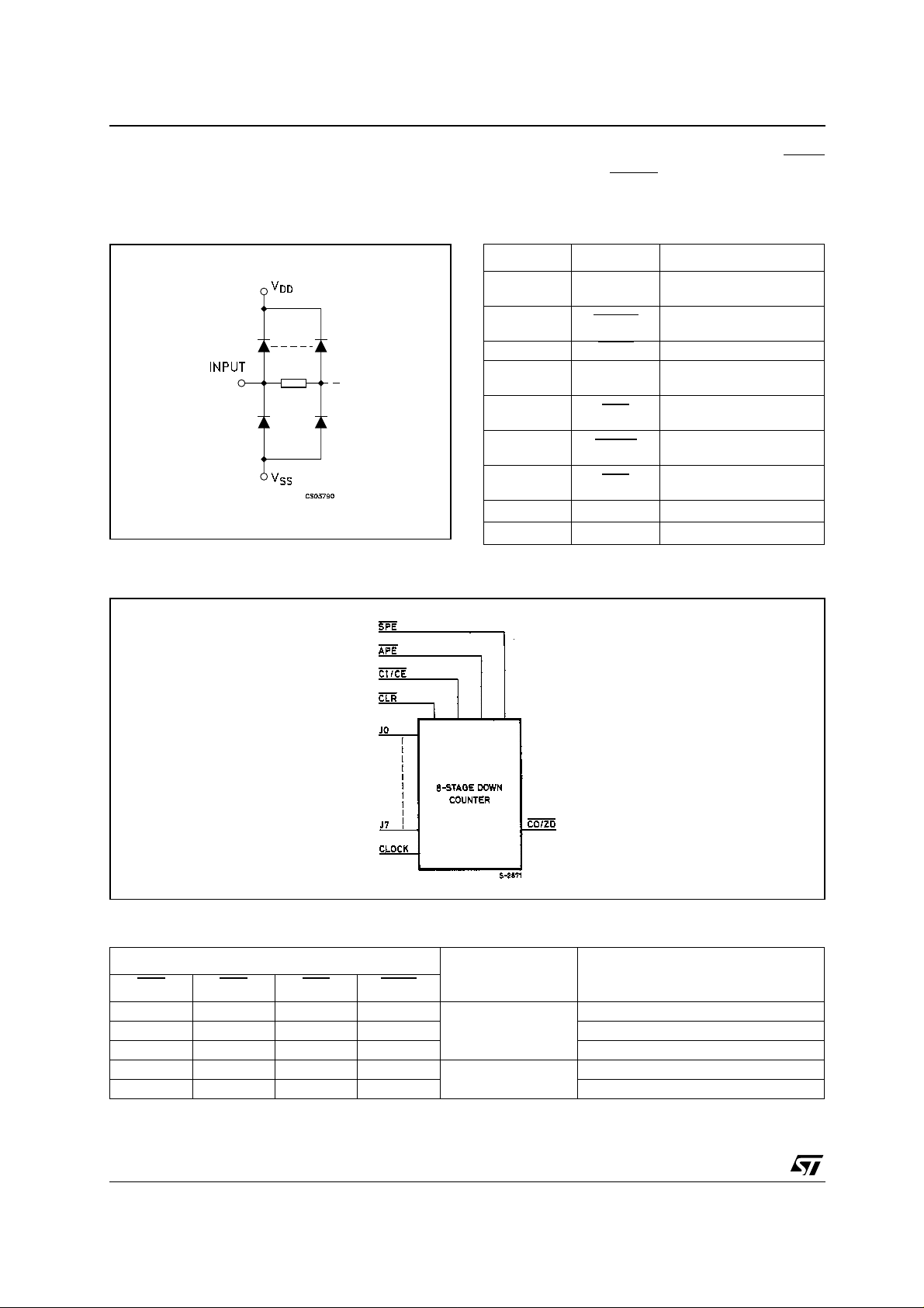
IINPUT EQUIVALENT CIRCUIT PIN DESCRIPTION
PIN No SYMBOL NAME AND FUNCTION
1 CLOCK
2 CLEAR
3 CI/CE
4, 5, 6, 7, 10,
11, 12, 13
9APE
14 CO/ZD
15 SPE
8
16
J0 to J7 Jam Inputs
V
V
FUNCTIONAL DIAGRAM
SS
DD
Clock Input (LOW to
HIGH edge triggered)
Asynchronous Master
Reset Input (Active Low)
Terminal Enable Input
Asynchronous Preset
Enable Inputs(Active Low)
Terminal Count Output
(Active Low)
Synchronous Preset
Enable Input (Active Low)
Negative Supply Voltage
Positive Supply Voltage
TRUTH TABLES
CONTROL INPUTS
CLR
HHHH
H H H L Count Down
H H L X Preset on Next Positive Clock Transition
HLXX
L X X X Clear to Maximum Count
X : Don’t Care
Clock connected t o Cl ock inpu t
Synchronous Operation : changes occur on negative to positive clock transitions.
2/14
APE SPE CI/CE
PRESET MODE ACTION
Inhibit Counter
Synchronous
Asynchronous
Preset Asynchronously
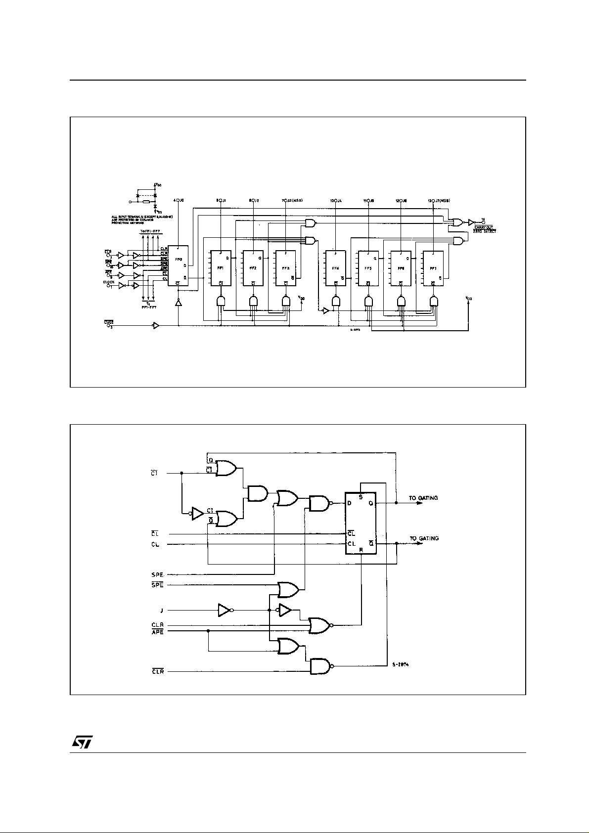
LOGIC DIAGRAM
HCF40103B
LOGIC DIAGRAM FOR FLIP-FLOPS, FF0-FF7
3/14
HCF40103B
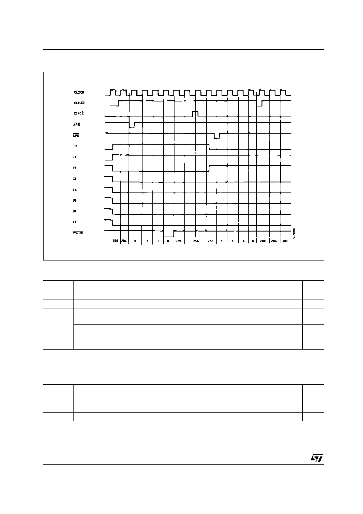
TIMING CHART
ABSOLUTE MAXIMUM RATINGS
Symbol Parameter Value Unit
V
V
P
Supply Voltage
DD
DC Input Voltage -0.5 to VDD + 0.5
I
I
DC Input Current
I
Power Dissipation per Package 200 mW
D
-0.5 to +22 V
10 mA
±
V
Power Dissipation per Output Transistor 100 mW
T
T
Absolute Maximum Ratings are those values beyond which damage to the device may occur. Functional operation under these conditions is
not implied.
All voltage value s are referred to V
Operating Temperature
op
Storage Temperature
stg
pin voltage.
SS
-55 to +125 °C
-65 to +150 °C
RECOMMENDED OPERATING CONDITIONS
Symbol Parameter Value Unit
V
V
T
Supply Voltage
DD
Input Voltage 0 to V
I
Operating Temperature
op
3 to 20 V
DD
-55 to 125 °C
V
4/14
DC SPECIFICATIONS
Test Condition Value
T
Symbol Parameter
I
Quiescent Current 0/5 5 0.04 5 150 150
L
V
(V)
V
I
(V)
|I
|
O
O
(µA)
V
DD
(V)
= 25°C
A
Min. Typ. Max. Min. Max. Min. Max.
0/10 10 0.04 10 300 300
0/15 15 0.04 20 600 600
0/20 20 0.08 100 3000 3000
V
High Level Output
OH
Voltage
0/5 <1 5 4.95 4.95 4.95
0/15 <1 15 14.95 14.95 14.95
Low Level Output
V
OL
Voltage
5/0 <1 5 0.05 0.05 0.05
15/0 <1 15 0.05 0.05 0.05
High Level Input
V
IH
Voltage
0.5/4.5 <1 5 3.5 3.5 3.5
1.5/13.5 <1 15 11 11 11
V
IL
Low Level Input
Voltage
4.5/0.5 <1 5 1.5 1.5 1.5
13.5/1.5 <1 15 4 4 4
I
OH
Output Drive
Current
0/5 2.5 <1 5 -1.36 -3.2 -1.1 -1.1
0/5 4.6 <1 5 -0.44 -1 -0.36 -0.36
0/10 9.5 <1 10 -1.1 -2.6 -0.9 -0.9
0/15 13.5 <1 15 -3.0 -6.8 -2.4 -2.4
I
OL
Output Sink
Current
0/5 0.4 <1 5 0.44 1 0.36 0.36
0/15 1.5 <1 15 3.0 6.8 2.4 2.4
Input Leakage
I
I
Current
C
Input Capacitance
I
The Noi se Margin for both "1" a nd "0" level is: 1V min. wit h VDD=5V, 2V min. with VDD=10V, 2.5V min. with VDD=15V
0/18 Any Input 18
Any Input 5 7.5 pF
-5
10
±
-40 to 85°C -55 to 125°C
0.1
±
1
±
HCF40103B
Unit
A
µ
V0/10 <1 10 9.95 9.95 9.95
V10/0 <1 10 0.05 0.05 0.05
V1/9 <1 10 7 7 7
V9/1 <1 10 3 3 3
mA
mA0/10 0.5 <1 10 1.1 2.6 0.9 0.9
1
±
A
µ
5/14

HCF40103B
DYNAMIC ELECTRICAL CHARACTERISTICS (T
Symbol Parameter
t
PHL tPLH
t
PHL tPLH
Propagation Delay Time
Clock To Out
Propagation Delay Time
Carry In/counter Enable To
Output
t
PHL tPLH
Propagation Delay Time
Asynchronous Preset
Enable To Output
t
PHL tPLH
t
THL tTLH
t
setup
t
setup
(*) Typical temper at ure coeffic i ent for all VDD value is 0.3 %/°C.
Propagation Delay Time
To Output
Clear
Transition Time 5 100 200
Clock Pulse Width 5 300 150
t
W
Clear Pulse Width 5 320 160
t
W
APE Pulse Width 5 360 180
t
W
SPE Setup Time 5 280 140
JAM Setup Time 5 200 100
Maximum Clock Input
f
CL
Frequency
(V)
V
DD
5 300 600
15 95 190
5 200 400
15 65 130
5 650 1300
15 200 400
5 375 750
15 100 200
15 40 80
15 80 40
15 100 50
15 120 60
15 100 50
15 60 30
5 0.7 1.4
15 2.4 4.8
= 25°C, CL = 50pF, RL = 200KΩ, tr = tf = 20 ns)
amb
Test Condition Value (*) Unit
Min. Typ. Max.
ns10 130 260
ns10 90 180
ns10 300 600
ns10 180 360
ns10 50 100
ns10 180 90
ns10 160 80
ns10 160 80
ns10 140 70
ns10 80 40
MHz10 1.8 3.6
6/14

TYPICAL APPLICATIONS
HCF40103B
DIVIDE BY "N" COUNTER
MICROPROCESSOR INTERRUPT TIMER
SYNCHRONOUS CASCADING
SYNCHRONOUS CASCADING
MICROPROCESSOR INTERRUPT TIMER
* An Output spike (160ns at VDD = 5V) occurs whenever tw o or
more devices are ca scaded in the parallel clocked mode because
the clock-to-carry out delay is greater than the carry-in-to-carry-out
delay . Thi s spik e is elimi nat ed by gati ng th e out put of th e last devi ce
with the clock as shown.
7/14

HCF40103B
TEST CIRCUIT
CL = 50pF or equivalent (in cl udes jig and probe capac i tance)
= 200K
R
R
Ω
L
= Z
of pulse generator (typically 50Ω)
T
OUT
WAVEFORM 1 : PROPAGATION DELAY TIME (f=1MHz; 50% duty cycle)
8/14
HCF40103B
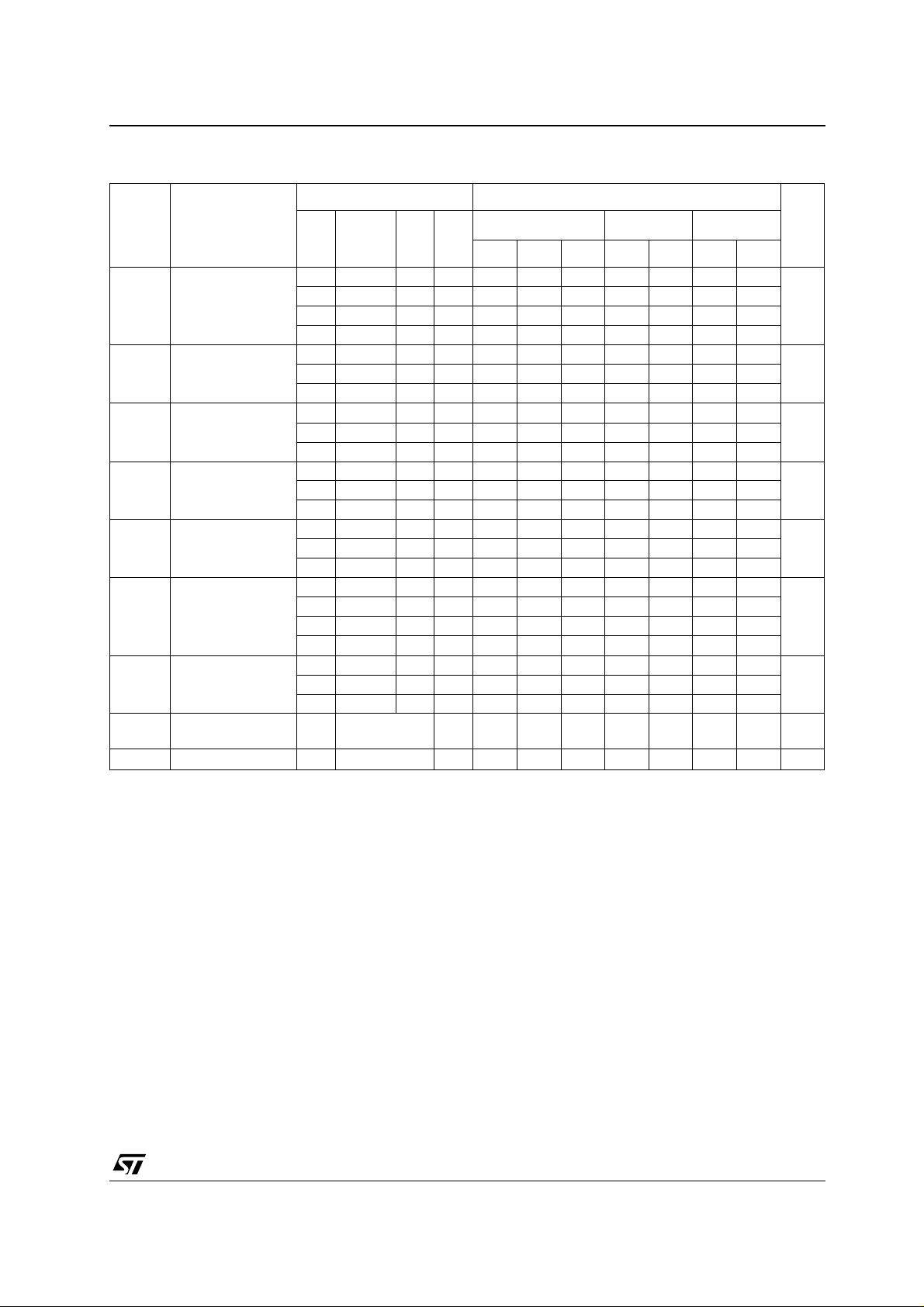
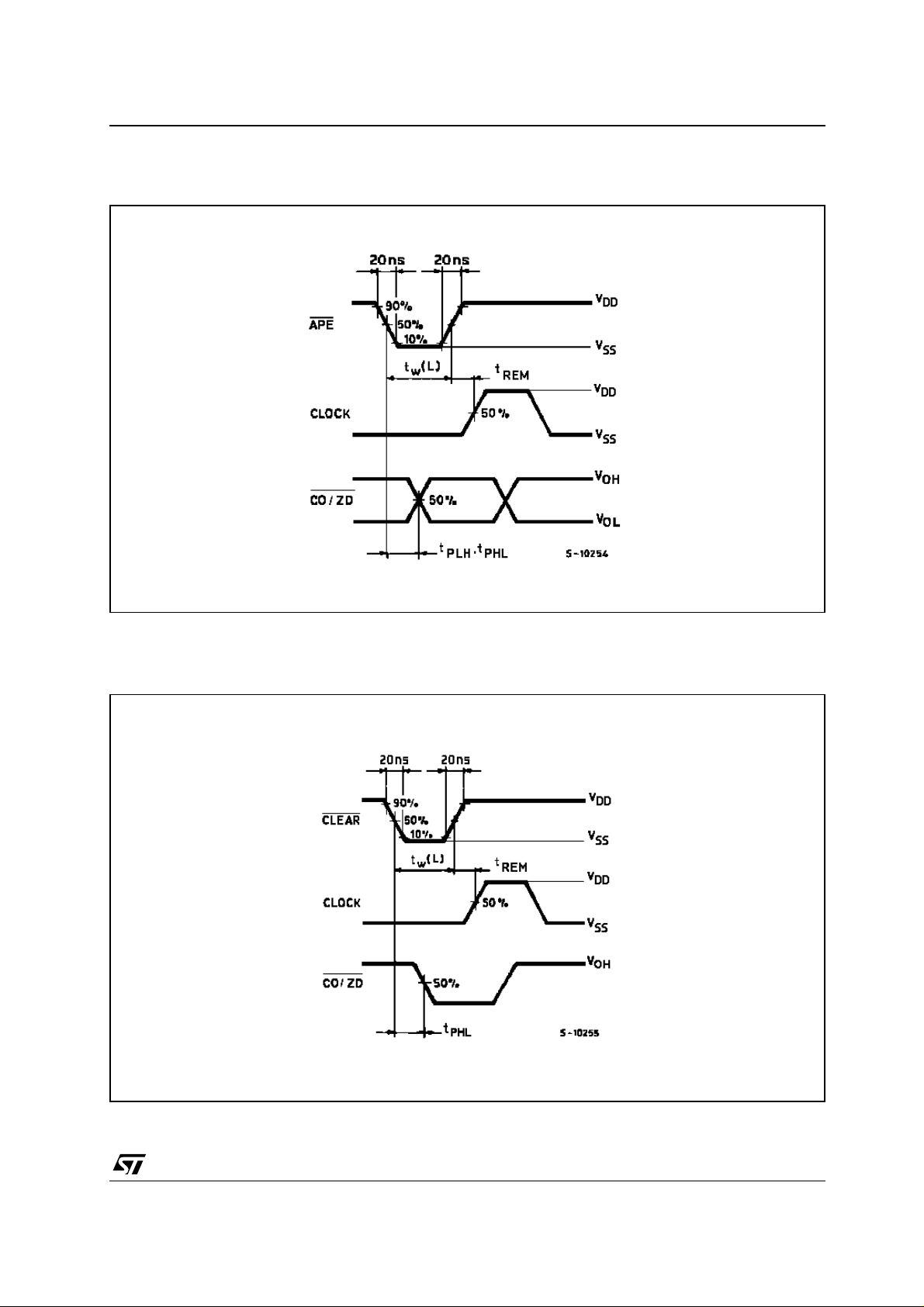
WAVEFORM 2 : PROPAGATION DELAY, MINIMUM PULSE WIDTH AND REMOVAL TIME (f=1MHz;
50% duty cycle)
WAVEFORM 3 : PROPAGATION DELAY, MINIMUM PULSE WIDTH AND REMOVAL TIME (f=1MHz;
50% duty cycle)
9/14

HCF40103B
WAVEFORM 4 : PROPAGATION DELAY TIME (f=1MHz; 50% duty cycle)
WAVEFORM 5 : MINIMUM SETUP TIME (f=1MHz; 50% duty cycle)
10/14

WAVEFORM 6 : MINIMUM SETUP TIME (f=1MHz; 50% duty cycle)
HCF40103B
11/14

HCF40103B
Plastic DIP-16 (0.25) MECHANICAL DATA
mm. inch
DIM.
MIN. TYP MAX. MIN. TYP. MAX.
a1 0.51 0.020
B 0.77 1.65 0.030 0.065
b 0.5 0.020
b1 0.25 0.010
D 20 0.787
E 8.5 0.335
e 2.54 0.100
e3 17.78 0.700
F 7.1 0.280
I 5.1 0.201
L 3.3 0.130
Z 1.27 0.050
12/14
P001C

SO-16 MECHANICAL DATA
HCF40103B
DIM.
A 1.75 0.068
a1 0.1 0.2 0.003 0.007
a2 1.65 0.064
b 0.35 0.46 0.013 0.018
b1 0.19 0.25 0.007 0.010
C 0.5 0.019
c1 45˚ (typ.)
D 9.8 10 0.385 0.393
E 5.8 6.2 0.228 0.244
e 1.27 0.050
e3 8.89 0.350
F 3.8 4.0 0.149 0.157
G 4.6 5.3 0.181 0.208
L 0.5 1.27 0.019 0.050
M 0.62 0.024
S ˚ (max.)
MIN. TYP MAX. MIN. TYP. MAX.
mm. inch
8
PO13H
13/14

HCF40103B
Information furnished is believed to be accurate and reliable. However, STMicroelectronics assumes no responsibility for the
consequences of use of such informatio n nor for any infringement of paten ts or o ther rig hts of t hird part ies which ma y result from
its use. No license is granted by implication or otherwise under any patent or patent rights of STMicroelectronics. Specifications
mentioned in this publication are subject to change without notice. This publication supersedes and replaces all information
previousl y suppl ied. STM icroel ectronics produc ts are not auth orized for use as c ritica l compone nts in l ife s upport dev ices or
systems without express written approval of STMicroelectronics.
Australia - Brazil - Canada - China - Finland - France - Germany - Hong Kong - India - Israel - Italy - Japan - Malaysia - Malta - Morocco
© The ST logo is a registered trademark of STMicroelectronics
© 2002 STMicroelectronics - Printed in Italy - All Rights Reserved
STMicroelectronics GROUP OF COMPANIES
Singapore - Spain - Sweden - Switzerland - United Kingdom - United States.
© http://www.st.com
14/14
 Loading...