

ST HCF4007UB User Manual
DUAL COMPLEM ENTARY PAIR PLUS INVERTER
■ STANDARDIZED SYMMETRICAL OUTPUT
CHARACTERISTICS
■ MEDIUM SPEED OPERATION
t
= 30ns (Typ.) AT 10V
PD
■ QUIESCENT CURRENT SPECIFIED UP TO
20V
■ 5V,10V AND 15V PARAMETRIC RATINGS
■ INPUT LEAKAGE CURRE NT
I
= 100nA (MAX) AT VDD=18VTA= 25°C
I
■ 100% TESTED FOR QUIESCENT CURRENT
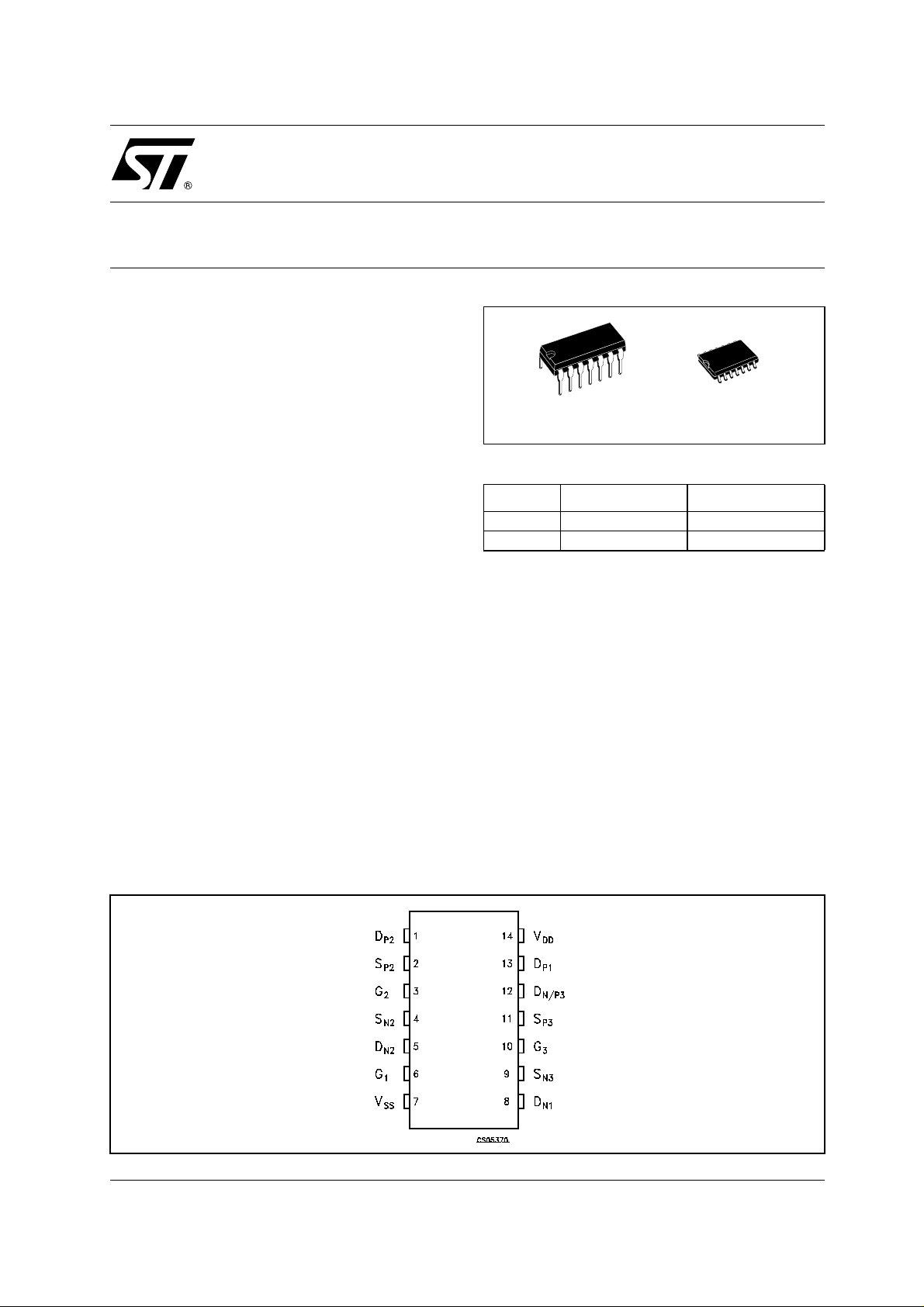
DESCRIPTION
The HCF4007UB is a monolithic integrated circuit
fabricated in Metal Oxide Semiconductor
technology available in DIP and SOP packages.
The HCF4007UB type is comprised of three
n-channel and three p-chan nel enhancement type
MOS transistors. The transistor elements are
accessible through the package terminals to
provide a convenient means for constructing the
various typical circuits as shown in typical
HCF4007UB
DIP SOP
ORDER CODES
PACKAGE TUBE T & R
DIP HCF4007UBEY
SOP HCF4007UBM1 HCF4007UM013TR
applications. More complex f unc tions are possible
using multiple packages. Number shown in
parentheses indicate termin als that are connected
together to form the various configuration listed.
PIN CONNECTION
1/9March 2004
HCF4007UB
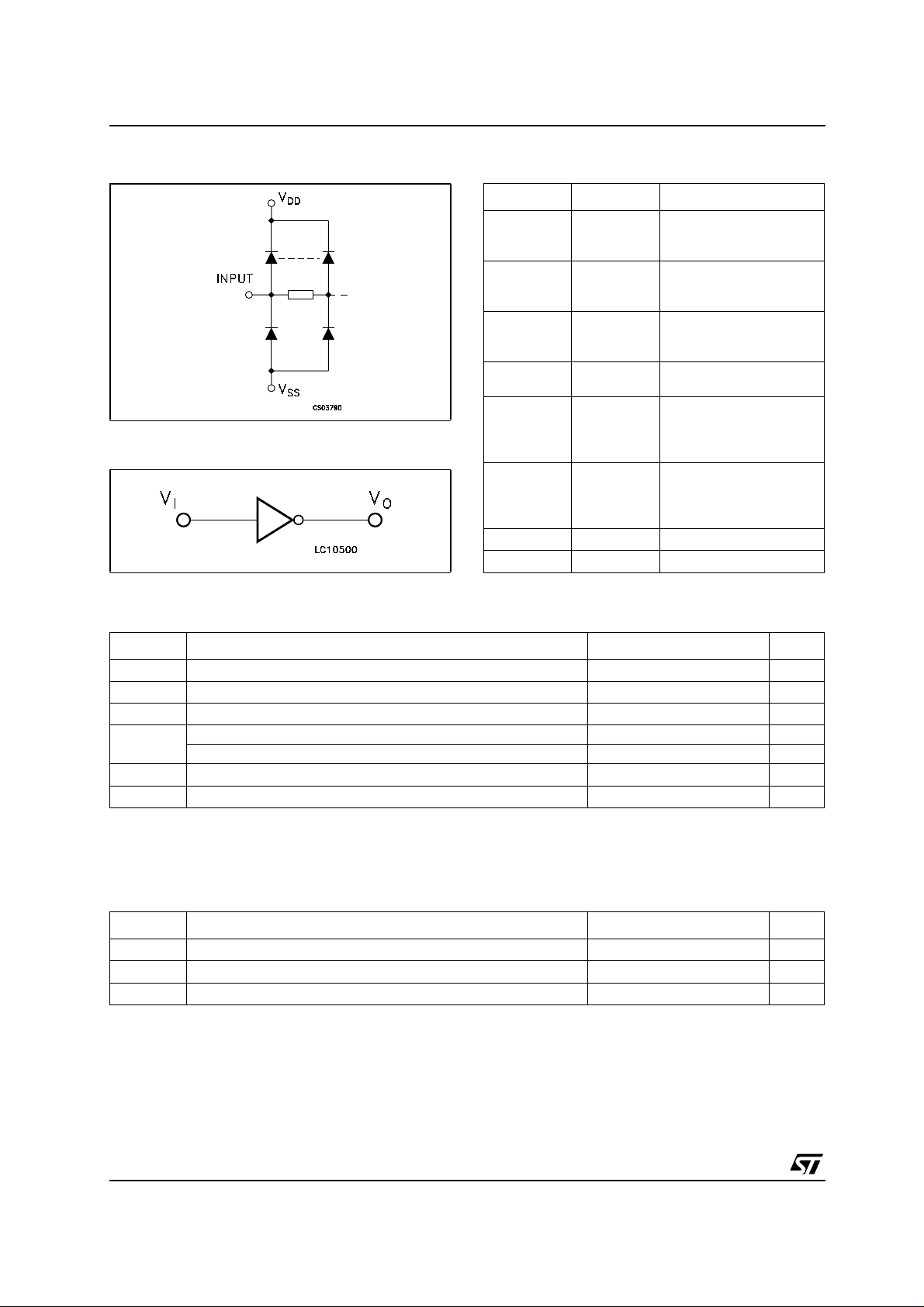
INPUT EQUIVALENT CIRCUIT
LOGIC DIAGRAM
ABSOLUTE MAXIMUM RATINGS
PIN DESCRIPTION
PIN N° SYMBOL NAME AND FUNCTION
Source Connections to
2nd and 3rd p-channel
transistors
Drain Connections from
the 1st and 2nd p-channel
transistors
Drain Connections from
the 1st and 2nd n-channel
transistors
Source Connections to
the 2nd and 3rdn-channel
Commonconnectionto
the 3rd p-channel and
n-channel transistor
drains
Gate connections to
n-channel and p-channel
3
of the three transistor
pairs
Negative Supply Voltage
Positive Supply Voltage
2, 11
13, 1
8, 5
4, 9
12
6, 3, 10
7
14
S
P2,SP3
D
P1,DP2
D
N1,DN2
S
N2,SN3
D
N/P3
G
1
V
V
to G
SS
DD
Symbol Parameter Value Unit
V
V
P
Supply Voltage
DD
DC Input Voltage -0.5 to VDD+0.5
I
DC Input Current
I
I
Power Dissipation per Package 200 mW
D
-0.5 to +22 V
± 10 mA
V
Power Dissipation per Output Transistor 100 mW
T
T
stg
Absolute Maximum Ratings are those values beyond which damage to the device may occur. Functional operation under these conditions is
not implied.
All voltagevalues are referredto V
Operating Temperature
op
Storage Temperature
pin voltage.
SS
-55 to +125 °C
-65 to +150 °C
RECOMMENDED OPERATING CONDITIONS
Symbol Parameter Value Unit
V
V
T
Supply Voltage
DD
Input Voltage 0 to V
I
Operating Temperature
op
3to20 V
DD
-55 to 125 °C
V
2/9
DC SPECIFICATIONS
Test Condition Value
T
Symbol Parameter
I
Quiescent Current 0/5 5 0.01 0.25 7.5 7.5
L
V
(V)
V
I
(V)
|I
|
O
O
(µA)
V
DD
(V)
= 25°C
A
Min. Typ. Max. Min. Max. Min. Max.
0/10 10 0.01 0.5 15 15
0/15 15 0.01 1 30 30
0/20 20 0.02 5 150 150
V
High Level Output
OH
Voltage
0/5 <1 5 4.95 4.95 4.95
0/15 <1 15 14.95 14.95 14.95
V
Low Level Output
OL
Voltage
5/0 <1 5 0.05 0.05 0.05
15/0 <1 15 0.05 0.05 0.05
V
High Level Input
IH
Voltage
0.5/4.5 <1 5 4 4 4
1.5/13.5 <1 15 12.5 12.5 12.5
V
Low Level Input
IL
Voltage
4.5/0.5 <1 5 1 1 1
13.5/1.5 <1 15 2.5 2.5 2.5
I
OH
Output Drive
Current
0/5 2.5 <1 5 -1.36 -3.2 -1.15 -1.1
0/5 4.6 <1 5 -0.44 -1 -0.36 -0.36
0/10 9.5 <1 10 -1.1 -2.6 -0.9 -0.9
0/15 13.5 <1 15 -3.0 -6.8 -2.4 -2.4
I
OL
Output Sink
Current
0/5 0.4 <1 5 0.44 1 0.36 0.36
0/15 1.5 <1 15 3.0 6.8 2.4 2.4
I
Input Leakage
I
Current
Input Capacitance
C
I
The NoiseMarginfor both "1"and "0"level is:1Vmin. withVDD=5V, 2V min. with VDD=10V, 2.5V min. with VDD=15V
0/18 Any Input 18
Any Input 5 7.5 pF
±10
-5
-40 to 85°C -55 to 125°C
±0.1 ±1 ±1 µA
HCF4007UB
Unit
µA
V0/10 <1 10 9.95 9.95 9.95
V10/0 <1 10 0.05 0.05 0.05
V1/9 <1 10 8 8 8
V9/1 <1 10 2 2 2
mA
mA0/10 0.5 <1 10 1.1 2.6 0.9 0.9
DYNAMIC ELECTRICAL CHARACTERISTICS (T
Symbol Parameter
t
PLHtPHL
t
TLHtTHL
(*) Typical temperature coefficient for all VDDvalue is 0.3%/°C.
Propagation Delay Time 5 55 110
Transition Time 5 100 200
(V)
V
DD
15 25 50
15 40 80
= 25°C, CL= 50pF, RL= 200KΩ,tr=tf=20ns)
amb
Test Condition Value (*) Unit
Min. Typ. Max.
ns10 30 60
ns10 50 100
3/9
 Loading...