

Page 1
Rad-hard high voltage CMOS logic series
Features
■ 3 to 20 V max operating voltage
■ Bufferized inputs and outputs
■ Standardized symmetrical outputs
characteristic
■ 50 ns typical propagation delays
■ 100 nA max 25 °C input current
■ 100% tested 20 V quiescent current
■ 5-10-15 V parametric testing
■ Hermetic packages
■ Rad-hard 100 kRad TID at 11rad/sec dose rate
■ SEL-SEU immune to 72 MeV/cm²/mg LET ions
■ ESCC qualified
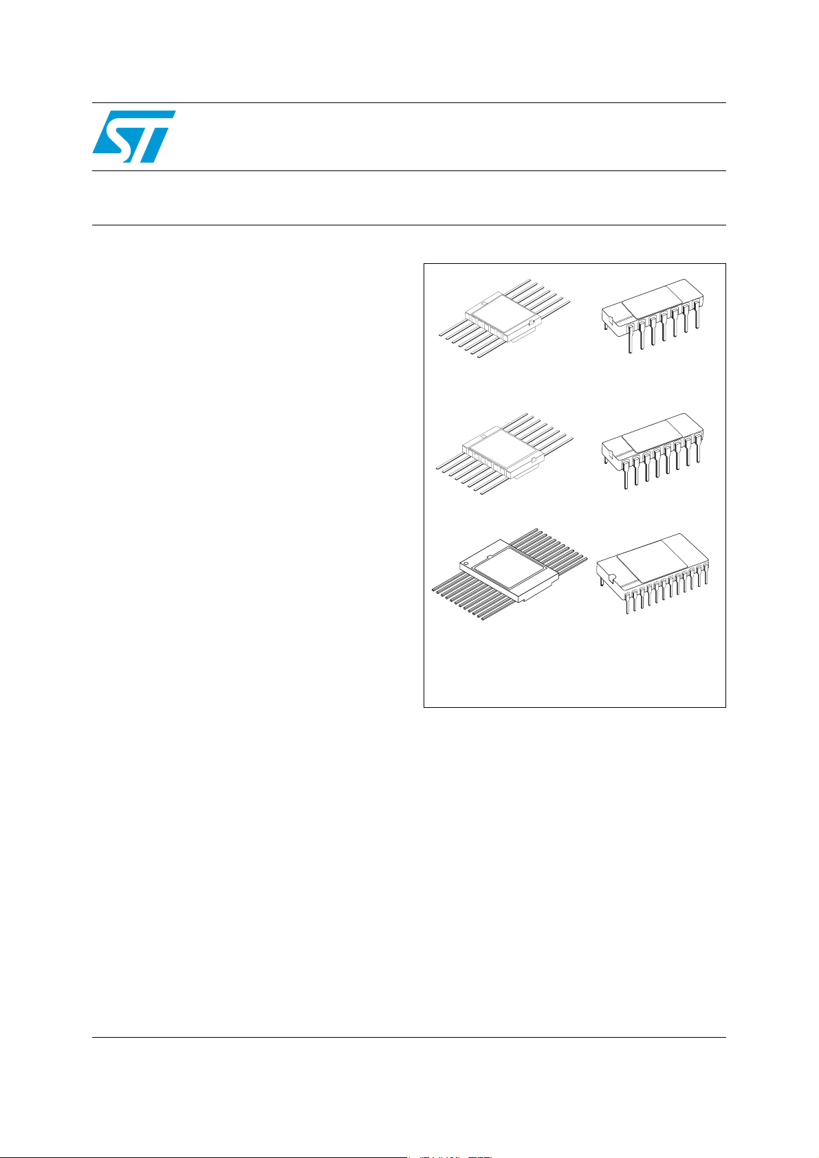
Flat-14
Flat-16
HCC40xxx
HCC45xxx
DIL-14
DIL-16
Description
The HCC40xxx and HCC45xxx series are
composed of over 70 types of high voltage CMOS
functions, offering a set of highly noise tolerant
gates, Flip-Flops, multiplexers, counters, bus
interfaces and several other functions. The
radiation hardness, the single event latch-up
(SEL) and the single event upset (SEU) immunity
and the housing in hermetic packages of all types
of both series make them usable in the most
difficult environmental conditions.
The complete specification of each type is
available from the European Space Components
Coordination web site (ESCC):
https://spacecomponents.org/. ST guarantees full
compliance of qualified parts with these ESCC
detailed specifications.
Flat-24
The upper metallic lid is not electrically connected to any
pins, nor to the IC die inside the package.
DIL-24
August 2011 Doc ID 17102 Rev 3 1/24
www.st.com
24
Page 2

Contents HCC4xxx
Contents
1 HCC family overview . . . . . . . . . . . . . . . . . . . . . . . . . . . . . . . . . . . . . . . . . 3
2 Input equivalent circuit diagram . . . . . . . . . . . . . . . . . . . . . . . . . . . . . . . 7
3 Maximum rating . . . . . . . . . . . . . . . . . . . . . . . . . . . . . . . . . . . . . . . . . . . . . 8
3.1 Recommended operating conditions . . . . . . . . . . . . . . . . . . . . . . . . . . . . . 8
4 Package mechanical data . . . . . . . . . . . . . . . . . . . . . . . . . . . . . . . . . . . . . 9
5 Order codes . . . . . . . . . . . . . . . . . . . . . . . . . . . . . . . . . . . . . . . . . . . . . . . 16
6 Revision history . . . . . . . . . . . . . . . . . . . . . . . . . . . . . . . . . . . . . . . . . . . 23
2/24 Doc ID 17102 Rev 3
Page 3
1 HCC family overview
HCC4xxx HCC family overview
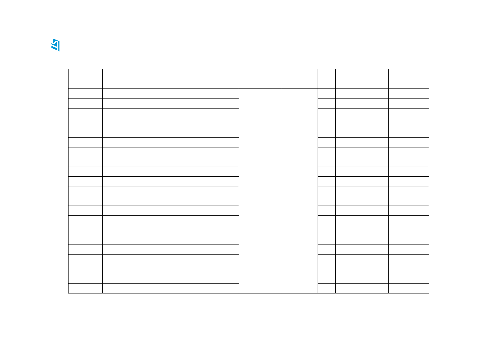
Table 1. Device summary
Part number Description Radiation level
HCC4001B Rad-hard quad 2-input NOR gate
HCC4002B Rad-hard dual 4-input NOR gate - 9201/042 Flat-14 - DIL-14
HCC4008B Rad-hard 4-bit full adder - 9202/039 Flat-16 - DIL-16
HCC4011B Rad-hard quad 2-input NAND gate Y 9201/043 Flat-14 - DIL-14
HCC4012B Rad-hard dual 4-input NAND gate - 9201/044 Flat-14 - DIL-14
Doc ID 17102 Rev 3 3/24
HCC4013B Rad-hard dual D Flip-Flop Y 9203/023 Flat-14 - DIL-14
HCC4014B Rad-hard 8-stage static synchronous shift register Y 9306/014 Flat-16 - DIL-16
HCC4015B Rad-hard dual 4-stage static shift register Y 9306/015 Flat-16 - DIL-16
HCC4016B Rad-hard quad bilateral switch - 9202/050 Flat-14 - DIL-14
HCC4017B Rad-hard decade counter/divider Y 9204/020 Flat-16 - DIL-16
HCC4018B Rad-hard presettable divide-by N counter - 9204/021 Flat-16 - DIL-16
HCC4019B Rad-hard quad AND/OR select gate Y 9202/051 Flat-16 - DIL-16
HCC4020B Rad-hard 14-stage binary/ripple counter Y 9204/022 Flat-16 - DIL-16
HCC4021B Rad-hard 8-stage static shift register Y 9306/016 Flat-16 - DIL-16
Agency
qualification
100 krad (Si) ESCC
EPPL ESCC specification Package
Y 9201/041 Flat-14 - DIL-14
HCC4022B Rad-hard divide-by-8 counter/divider - 9204/023 Flat-16 - DIL-16
HCC4023B Rad-hard triple 3-input NAND gate Y 9201/045 Flat-14 - DIL-14
HCC4024B Rad-hard 7-stage binary/ripple counter Y 9204/024 Flat-14 - DIL-14
HCC4025B Rad-hard triple 3-input NOR gate - 9201/046 Flat-14 - DIL-14
HCC4027B Rad-hard dual J-K master-slave Flip-Flop Y 9203/022 Flat-16 - DIL-16
HCC4028B Rad-hard BCD-to-decimal decoder Y 9205/010 Flat-16 - DIL-16
HCC4029B Rad-hard presettable up/down counter Y 9204/025 Flat-16 - DIL-16
Page 4
4/24 Doc ID 17102 Rev 3
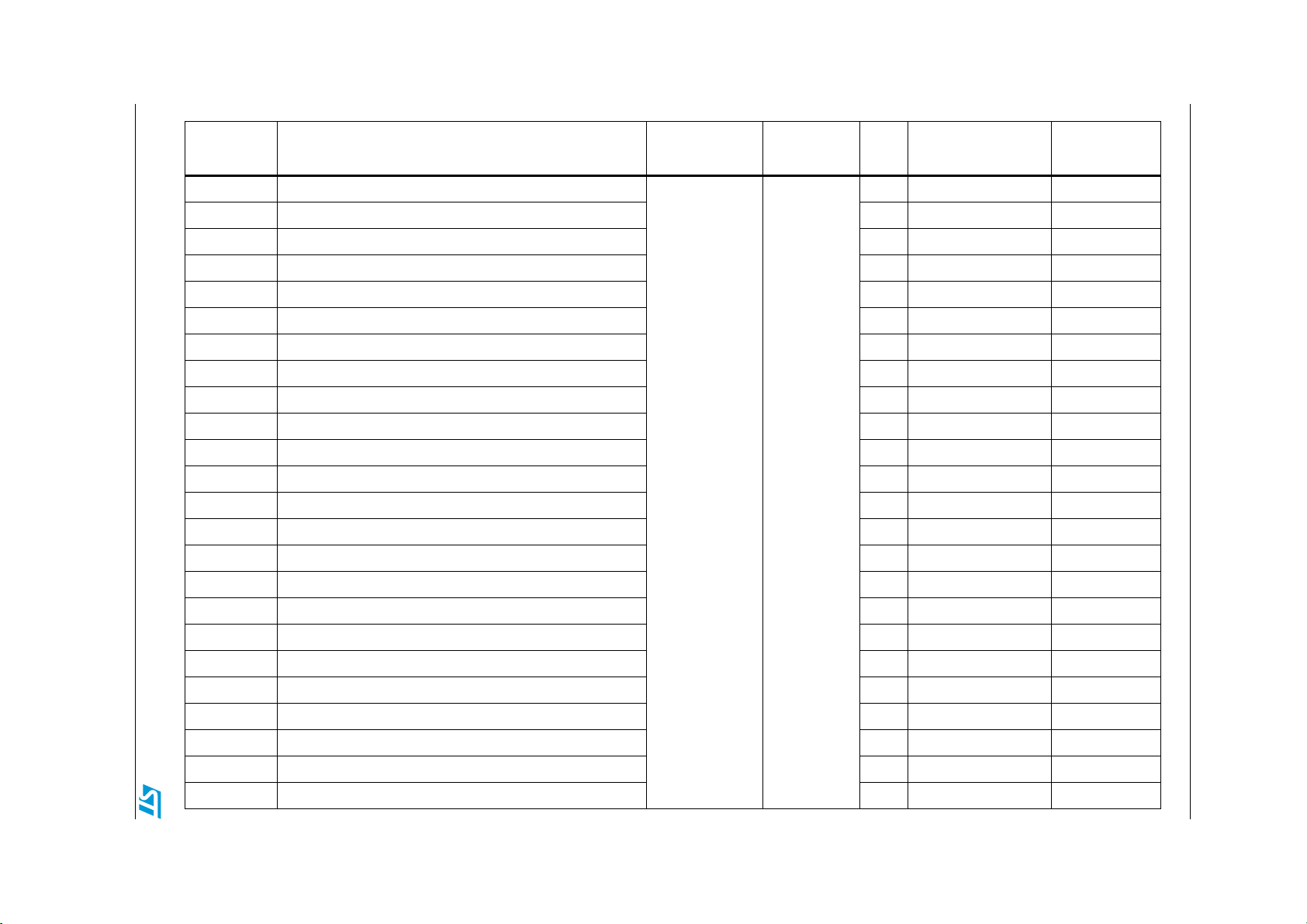
Table 1. Device summary (continued)
HCC family overview HCC4xxx
Part number Description Radiation level
HCC4030B Rad-hard quad exclusive OR gate
HCC4034B Rad-hard 8-stage static bidirectional bus register - 9306/025 Flat-24 - DIL-24
HCC4035B Rad-hard 4-stage parallel I/O shift register Y 9306/018 Flat-16 - DIL-16
HCC4040B Rad-hard 12-stage binary/ripple counter Y 9204/026 Flat-16 - DIL-16
HCC4041UB Rad-hard quad true/complement buffer - 9202/040 Flat-14 - DIL-14
HCC4042B Rad-hard quad clocked D latch - 9202/041 Flat-16 - DIL-16
HCC4043B Rad-hard quad 3-state NOR R/S latch - 9202/042 Flat-16 - DIL-16
HCC4044B Rad-hard quad 3-state NAND R/S latch - 9202/043 Flat-16 - DIL-16
HCC4046B Rad-hard micropower phase locker loop - 9202/044 Flat-16 - DIL-16
HCC4047B Rad-hard monostable/astable multivibrator Y 9207/003 Flat-14 - DIL-14
HCC4049UB Rad-hard hex inverting buffer/converter Y 9202/045 Flat-16 - DIL-16
HCC4050B Rad-hard hex non-inverting buffer/converter Y 9202/046 Flat-16 - DIL-16
100 krad (Si) ESCC
HCC4051B Rad-hard single 8-channel analog mux/demux Y 9202/047 Flat-16 - DIL-16
HCC4052B Rad-hard different 4-channel analog mux/demux - 9202/048 Flat-16 - DIL-16
HCC4053B Rad-hard triple 2-channel analog mux/demux - 9202/049 Flat-16 - DIL-16
HCC4060B Rad-hard 14-stage counter/divider AND oscillator - 9204/052 Flat-16 - DIL-16
HCC4063B Rad-hard 4-bit magnitude comparator Y 9209/001 Flat-16 - DIL-16
Agency
qualification
EPPL ESCC specification Package
Y 9201/047 Flat-14 - DIL-14
HCC4066B Rad-hard quad bilateral switch Y 9408/005 Flat-14 - DIL-14
HCC4067B Rad-hard single 16-channel analog mux/demux - 9408/009 Flat-24 - DIL-24
HCC4068B Rad-hard 8-input NAND/AND gate - 9201/061 Flat-14 - DIL-14
HCC4069UB Rad-hard hex inverter Y 9401/010 Flat-14 - DIL-14
HCC4070B Rad-hard quad exclusive OR gate - 9201/048 Flat-14 - DIL-14
HCC4071B Rad-hard quad 2-input OR gate Y 9201/063 Flat-14 - DIL-14
HCC4072B Rad-hard dual 4-input OR gate - 9201/082 Flat-14 - DIL-14
Page 5
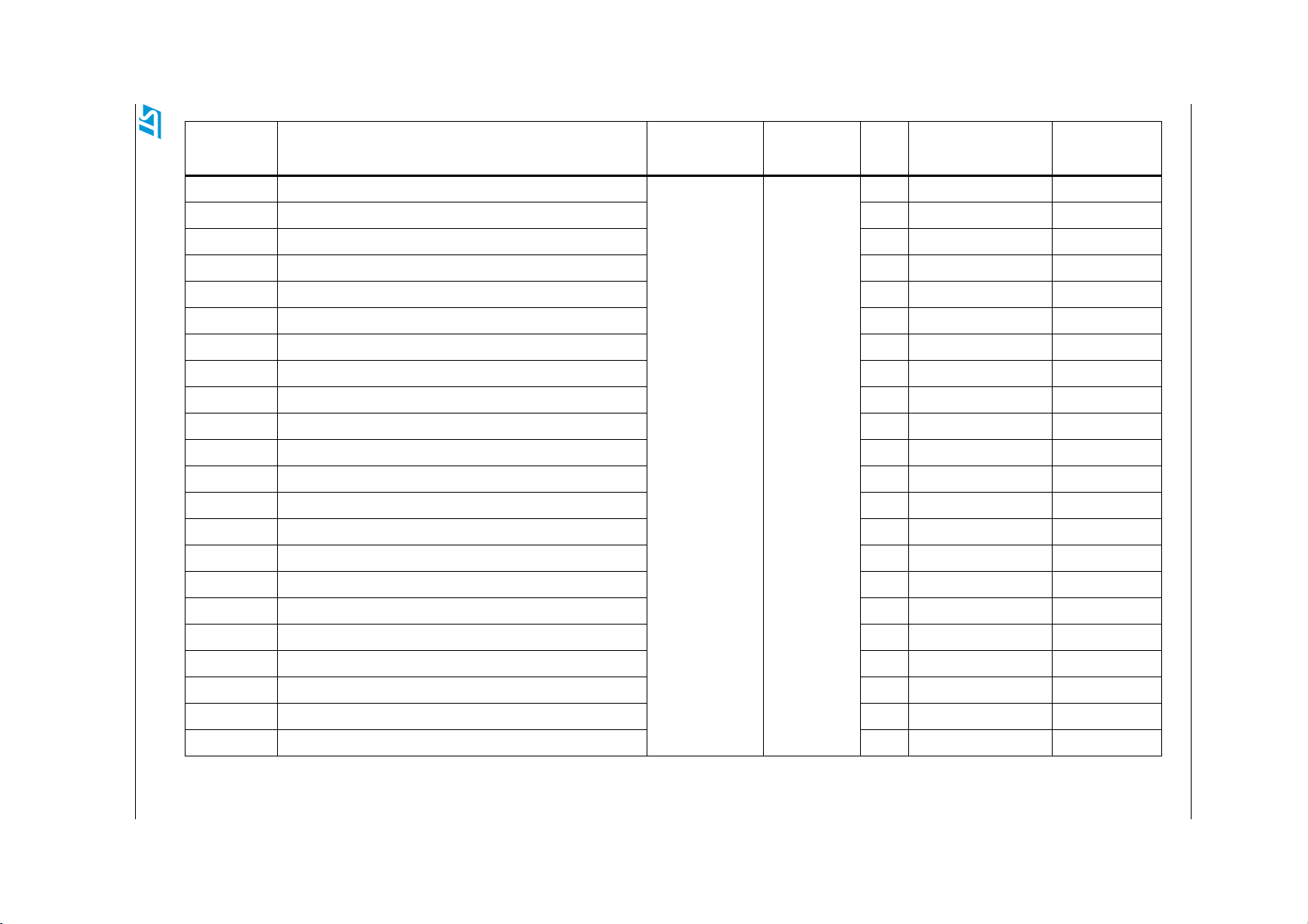
Table 1. Device summary (continued)
HCC4xxx HCC family overview
Doc ID 17102 Rev 3 5/24
Part number Description Radiation level
HCC4073B Rad-hard triple 3-input AND gate
HCC4075B Rad-hard triple 3-input OR gate - 9201/065 Flat-14 - DIL-14
HCC4076B Rad-hard 4-bit D-type register Y 9306/022 Flat-16 - DIL-16
HCC4077B Rad-hard quad exclusive NOR gate - 9201/055 Flat-14 - DIL-14
HCC4078B Rad-hard 8-input NOR/OR gate - 9201/062 Flat-14 - DIL-14
HCC4081B Rad-hard quad 2-input AND gate Y 9201/052 Flat-14 - DIL-14
HCC4082B Rad-hard dual 4-input AND gate - 9201/066 Flat-14 - DIL-14
HCC4093B Rad-hard quad 2-input NAND Schmitt trigger Y 9409/002 Flat-14 - DIL-14
HCC4094B Rad-hard 8-stage shift-and-store bus register Y 9306/026 Flat-16 - DIL-16
HCC4098B Rad-hard dual monostable multivibrator - 9206/002 Flat-16 - DIL-16
HCC4099B Rad-hard 8-bit addressable latch Y 9202/058 Flat-16 - DIL-16
100 krad (Si) ESCC
HCC40103B Rad-hard presettable 8-bit binary down counter Y 9204/036 Flat-16 - DIL-16
HCC40106B Rad-hard hex schmitt trigger Y 9409/005 Flat-14 - DIL-14
HCC40107B Rad-hard dual 2-input NAND buffer/driver Y 9401/013 Flat-14 - DIL-14
HCC40109B Rad-hard quad low-to-high voltage level shifter Y 9407/003 Flat-16 - DIL-16
HCC40161B Rad-hard binary counter with asynchronous clear Y 9204/054 Flat-16 - DIL-16
HCC40174B Rad-hard hex D Flip-Flop Y 9203/038 Flat-16 - DIL-16
Agency
qualification
EPPL ESCC specification Package
Y 9201/064 Flat-14 - DIL-14
HCC40193B Rad-hard presettable 4-bit binary up-down counter - 9204/041 Flat-16 - DIL-16
HCC4502B Rad-hard strobed hex inverter/buffer Y 9401/006 Flat-16 - DIL-16
HCC4503B Rad-hard hex buffer 3-state non-inverter Y 9401/030 Flat-16 - DIL-16
HCC4508B Rad-hard dual 4-bit Latch 3-state outputs Y 9202/063 Flat-24 - DIL-24
HCC4512B Rad-hard 8-channel data selec. with 3-state output Y 9408/006 Flat-16 - DIL-16
Page 6
6/24 Doc ID 17102 Rev 3
Table 1. Device summary (continued)
HCC family overview HCC4xxx
Part number Description Radiation level
HCC4514B Rad-hard 4-bit Latch / 4-to-16 line decoder output high
HCC4515B Rad-hard 4-bit Latch / 4-to-16 line decoder output low - 9205/011 Flat-24 - DIL-24
HCC4516B Rad-hard presettable 4-bit binary up/down counter - 9204/045 Flat-16 - DIL-16
HCC4520B Rad-hard dual binary up-down counter - 9204/028 Flat-16 - DIL-16
100 krad (Si) ESCC
HCC4532B Rad-hard 8-input priority encoder - 9202/065 Flat-16 - DIL-16
HCC4538B Rad-hard dual precision monostable multivibrator - 9207/007 Flat-16 - DIL-16
HCC4555B Rad-hard dual 1-of-4 decoder/demux output high Y 9408/011 Flat-16 - DIL-16
HCC4556B Rad-hard dual 1-of-4 decoder/demux output low - 9408/025 Flat-16 - DIL-16
Agency
qualification
EPPL ESCC specification Package
- 9408/012 Flat-24 - DIL-24
Note: Contact ST sales office for information about the specific conditions for other CMOS4000 part numbers and product in die form
Page 7
HCC4xxx Input equivalent circuit diagram
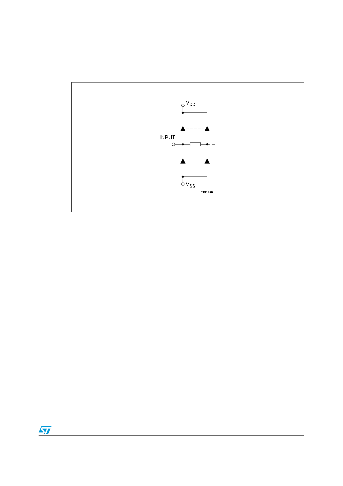
2 Input equivalent circuit diagram
Figure 1. Input equivalent circuit diagram
Doc ID 17102 Rev 3 7/24
Page 8
Maximum rating HCC4xxx
3 Maximum rating
Stressing the device above the rating listed in the “absolute maximum ratings” table may
cause permanent damage to the device. These are stress ratings only and operation of the
device at these or any other conditions above those indicated in the operating sections of
this specification is not implied. Exposure to absolute maximum rating conditions for
extended periods may affect device reliability.
Table 2. Absolute maximum ratings
Symbol Parameter Value Unit
V
P
T
T
Supply voltage -0.5 to 22 V
DD
DC input voltage -0.5 to VDD + 0.5 V
V
I
I
DC input current ±10 mA
I
Power dissipation per package 200 mW
D
Operating temperature -55 to +125 °C
OP
Storage temperature -65 to +150 °C
STG
Note: All voltage values are referred to VSS pin voltage.
3.1 Recommended operating conditions
Table 3. Recommended operating conditions
Symbol Parameter Value Unit
V
V
T
Supply voltage 20 V
DD
Input voltage 0 to V
I
Operating temperature -55 to +125 °C
OP
DD
V
8/24 Doc ID 17102 Rev 3
Page 9

HCC4xxx Package mechanical data
4 Package mechanical data
In order to meet environmental requirements, ST offers these devices in different grades of
ECOPACK
specifications, grade definitions and product status are available at: www.st.com.
ECOPACK is an ST trademark.
®
packages, depending on their level of environmental compliance. ECOPACK®
Doc ID 17102 Rev 3 9/24
Page 10

Package mechanical data HCC4xxx
Table 4. Ceramic Flat-14 mechanical data
mm
Dim
Min Typ Max
A 6.75 6.91 7.06
B 9.76 9.95 10.14
C 1.49 1.95
D 0.10 0.127 0.15
E 7.50 7.62 7.75
F 1.27
G 0.38 0.43 0.48
H 6.0
L 18.75 en 22.0
M 0.38
N 4.31
Figure 2. Ceramic Flat-14 mechanical drawings
F
H
A
1
H
E
B
G
814
7
D
N
M
L
C
016029E
Note: The upper metallic lid is not electrically connected to any pins, nor to the IC die inside the
package. Connecting unused pins or metal lid to ground or to the power supply will not affect
the electrical characteristics.
10/24 Doc ID 17102 Rev 3
Page 11

HCC4xxx Package mechanical data
Table 5. Ceramic DIL-14 mechanical data
Mm.
Dim.
Min. Typ Max.
A 2.1 2.54
a1 3.00 3.70
a2 0.63 0.88 1.14
B 1.82 2.03 2.39
b 0.40 0.45 0.50
b1 0.20 0.254 0.30
D 18.79 19.00 19.20
E 7.36 7.62 7.87
e 2.54
e1 15.11 15.24 15.37
e2 7.62 7.87 8.12
F 7.11 7.75
I 3.70
K 10.90 12.1 n
L 1.14 1.27 1.5
Figure 3. Ceramic DIL-14 mechanical drawings
0016173H
Note: The upper metallic lid is not electrically connected to any pins, nor to the IC die inside the
package. Connecting unused pins or metal lid to ground or to the power supply will not affect
the electrical characteristics.
Doc ID 17102 Rev 3 11/24
Page 12

Package mechanical data HCC4xxx
Table 6. Ceramic Flat-16 mechanical data
mm.
Dim.
Min. Typ Max.
A 6.75 6.91 7.06
B 9.76 9.94 10.14
C 1.49 1.95
D 0.102 0.127 0.152
E 8.76 8.89 9.01
F 1.27
G 0.38 0.43 0.48
H 6.0
L 18.75 en 22.0
M 0.33 0.38 0.43
N 4.31
Figure 4. Ceramic Flat-16 mechanical drawings
F
H
16
A
1
H
E
B
G
9
8
D
N
M
L
C
0016030E
Note: The upper metallic lid is not electrically connected to any pins, nor to the IC die inside the
package. Connecting unused pins or metal lid to ground or to the power supply will not affect
the electrical characteristics.
12/24 Doc ID 17102 Rev 3
Page 13

HCC4xxx Package mechanical data
Table 7. Ceramic DIL-16 package dimensions
mm
Dim
Min Typ Max
A 2.10 2.71
a1 3.00 3.70
a2 0.63 0.88 1.14
B 1.82 2.39
b 0.40 0.45 0.50
b1 0.20 0.254 0.30
D 20.06 20.32 20.58
E 7.36 7.62 7.87
e 2.54
e1 17.65 17.78 17.90
e2 7.62 7.87 8.12
F 7.29 7.49 7.70
I 3.83
K 10.90 12.10
L 1.14 1.50
Figure 5. Ceramic DIL-16 package drawings
Note: The upper metallic lid is not electrically connected to any pins, nor to the IC die inside the
package. Connecting unused pins or metal lid to ground or to the power supply will not affect
the electrical characteristics.
Doc ID 17102 Rev 3 13/24
Page 14

Package mechanical data HCC4xxx
Table 8. Ceramic Flat-24 package dimensions
mm
Dim
Min Typ Max
A 10.70 11.00 11.30
B 15.30 15.49 15.70
C 1.45 1.90
D 0.23 0.254 0.30
E 13.84 13.97 14.10
F 1.22 1.27 1.32
G 0.45 0.508 0.55
H 7.25 8.25
L 25.00 28.00
M 0.45 0.508 0.55
N 7.01
Figure 6. Ceramic Flat-24 package drawings
Note: The upper metallic lid is not electrically connected to any pins, nor to the IC die inside the
package. Connecting unused pins or metal lid to ground or to the power supply will not affect
the electrical characteristics.
14/24 Doc ID 17102 Rev 3
Page 15

HCC4xxx Package mechanical data
Table 9. Ceramic DIL-24 package dimensions
mm
Dim
Min Typ Max
A 2.159 1.931 2.387
a1 1.270 1.016 1.524
a2 0.307 0.274 0.340
B 1.270
b1 0.457 0.407 0.507
b2 .254 0.229 0.304
C 2.466 2.205 2.727
D 30.48 30.17 30.78
E 15.24 14.98 15.49
e 2.540 2.410 2.670
e3 27.94 27.81 28.06
F 15.11 14.85 15.36
K 12.80 12.60 13.00
K1 12.80 12.60 13.00
L 3.300 3.000 3.800
Figure 7. Ceramic DIL-24 package drawings
0016179I
Note: The upper metallic lid is not electrically connected to any pins, nor to the IC die inside the
package. Connecting unused pins or metal lid to ground or to the power supply will not affect
the electrical characteristics.
Doc ID 17102 Rev 3 15/24
Page 16

16/24 Doc ID 17102 Rev 3
5 Order codes
Table 10. Ordering information
Order code
ESCC detailed
specification
Quality level Comment Package Lead finish Marking
Mass
(g)
Order codes HCC4xxx
EPPL Packing
HCC4001BK 9201/041/01 or 02
HCC4001BD 9201/041/03 or 04 DIL-14 920104103 or 04 2.20 -
HCC4002BK 9201/042/01 or 02 Flat-14 920104201 or 02 0.70 -
HCC4002BD 9201/042/03 or 04 DIL-14 920104203 or 04 2.20 -
HCC4008BK 9202/039/01 or 02 Flat-16 920203901 or 02 0.70 -
HCC4008BD 9202/039/08 or 09 DIL-16 920203908 or 09 2.20 -
HCC4011BK 9201/043/01 or 02 Flat-14 920104301 or 02 0.70 Y
HCC4011BD 9201/043/03 or 04 DIL-14 920104303 or 04 2.20 -
HCC4012BK 9201/044/01 or 02 Flat-14 920104401 or 02 0.70 -
HCC4012BD 9201/044/03 or 04 DIL-14 920104403 or 04 2.20 -
HCC4013BK 9203/023/01 or 02 Flat-14 920302301 or 02 0.70 Y
ESCC flight Specify ESCC variant number in PO
HCC4013BD 9203/023/03 or 04 DIL-14 920302303 or 04 2.20 -
HCC4014BK 9306/014/01 or 02 Flat-16 930601401 or 02 0.70 Y
HCC4014BD 9306/014/08 or 09 DIL-16 930601408 or 09 2.20 -
HCC4015BK 9306/015/01 or 02 Flat-16 930601501 or 02 0.70 Y
HCC4015BD 9306/015/08 or 09 DIL-16 930601508 or 09 2.20 -
HCC4016BK 9202/050/01 or 02 Flat-14 920205001 or 02 0.70 -
HCC4016BD 9202/050/03 or 04 DIL-14 920205003 or 04 2.20 -
HCC4017BK 9204/020/01 or 02 Flat-16 920402001 or 02 0.70 Y
HCC4017BD 9204/020/08 or 09 DIL-16 920402008 or 09 2.20 -
HCC4018BK 9204/021/01 or 02 Flat-16 920402101 or 02 0.70 -
HCC4018BD 9204/021/08 or 09 DIL-16 920402108 or 09 2.20 -
Flat-14
920104101 or 02 0.70 Y
Gold or solder dip
Strip pack
Page 17

Table 10. Ordering information (continued)
Order code
ESCC detailed
specification
Quality level Comment Package Lead finish Marking
Mass
(g)
HCC4xxx Order codes
EPPL Packing
Doc ID 17102 Rev 3 17/24
HCC4019BK 9202/051/01 or 02
HCC4019BD 9202/051/08 or 09 DIL-16 920205108 or 09 2.20 -
HCC4020BK 9204/022/01 or 02 Flat-16 920402201 or 02 0.70 Y
HCC4020BD 9204/022/08 or 09 DIL-16 920402208 or 09 2.20 -
HCC4021BK 9306/016/01 or 02 Flat-16 930601601 or 02 0.70 Y
HCC4021BD 9306/016/08 or 09 DIL-16 930601608 or 09 2.20 -
HCC4022BK 9204/023/01 or 02 Flat-16 920402301 or 02 0.70 -
HCC4022BD 9204/023/08 or 09 DIL-16 920402308 or 09 2.20 -
HCC4023BK 9201/045/01 or 02 Flat-14 920104501 or 02 0.70 Y
HCC4023BD 9201/045/03 or 04 DIL-14 920104503 or 04 2.20 -
HCC4024BK 9204/024/01 or 02 Flat-14 920402401 or 02 0.70 Y
HCC4024BD 9204/024/03 or 04 DIL-14 920402403 or 04 2.20 -
HCC4025BK 9201/046/01 or 02 Flat-14 920104601 or 02 0.70 -
HCC4025BD 9201/046/03 or 04 DIL-14 920104603 or 04 2.20 -
HCC4027BK 9203/022/01 or 02 Flat-16 920302201 or 02 0.70 Y
HCC4027BD 9203/022/08 or 09 DIL-16 920302208 or 09 2.20 -
HCC4028BK 9205/010/01 or 02 Flat-16 920501001 or 02 0.70 Y
HCC4028BD 9205/010/08 or 09 DIL-16 920501008 or 09 2.20 -
HCC4029BK 9204/025/01 or 02 Flat-16 920402501 or 02 0.70 Y
HCC4029BD 9204/025/08 or 09 DIL-16 920402508 or 09 2.20 -
HCC4030BK 9201/047/01 or 02 Flat-14 920104701 or 02 0.70 Y
HCC4030BD 9201/047/03 or 04 DIL-14 920104703 or 04 2.20 -
HCC4034BK 9306/025/01 or 02 Flat-24 930602501 or 02 1.70 -
HCC4034BD 9306/025/03 or 04 DIL-24 930602503 or 04 5.20 -
HCC4035BK 9306/018/01 or 02 Flat-16 930601801 or 02 0.70 Y
ESCC flight Specify ESCC variant number in PO
Flat-16
920205101 or 02 0.70 Y
Gold or solder dip
Strip pack
Page 18

18/24 Doc ID 17102 Rev 3
Table 10. Ordering information (continued)
Order code
ESCC detailed
specification
Quality level Comment Package Lead finish Marking
Mass
(g)
Order codes HCC4xxx
EPPL Packing
HCC4035BD 9306/018/08 or 09
HCC4040BK 9204/026/01 or 02 Flat-16 920402601 or 02 0.70 Y
HCC4040BD 9204/026/08 or 09 DIL-16 920402608 or 09 2.20 -
HCC4041UBK 9202/040/01 or 02 Flat-14 920204001 or 02 0.70 -
HCC4041UBD 9202/040/03 or 04 DIL-14 920204003 or 04 2.20 -
HCC4042BK 9202/041/01 or 02 Flat-16 920204101 or 02 0.70 -
HCC4042BD 9202/041/08 or 09 DIL-16 920204108 or 09 2.20 -
HCC4043BK 9202/042/01 or 02 Flat-16 920204201 or 02 0.70 -
HCC4043BD 9202/042/08 or 09 DIL-16 920204208 or 09 2.20 -
HCC4044BK 9202/043/01 or 02 Flat-16 920204301 or 02 0.70 -
HCC4044BD 9202/043/08 or 09 DIL-16 920204308 or 09 2.20 -
HCC4046BK 9202/044/01 or 02 Flat-16 920204401 or 02 0.70 -
HCC4046BD 9202/044/08 or 09 DIL-16 920204408 or 09 2.20 -
HCC4047BK 9207/003/01 or 02 Flat-14 920700301 or 02 0.70 Y
HCC4047BD 9207/003/03 or 04 DIL-14 920700303 or 04 2.20 -
HCC4049UBK 9202/045/01 or 02 Flat-16 920204501 or 02 0.70 Y
HCC4049UBD 9202/045/08 or 09 DIL-16 920204508 or 09 2.20 -
HCC4050BK 9202/046/01 or 02 Flat-16 920204601 or 02 0.70 Y
HCC4050BD 9202/046/08 or 09 DIL-16 920204608 or 09 2.20 -
HCC4051BK 9202/047/01 or 02 Flat-16 920204701 or 02 0.70 Y
HCC4051BD 9202/047/08 or 09 DIL-16 920204708 or 09 2.20 -
HCC4052BK 9202/048/01 or 02 Flat-16 920204801 or 02 0.70 -
HCC4052BD 9202/048/08 or 09 DIL-16 920204808 or 09 2.20 -
HCC4053BK 9202/049/01 or 02 Flat-16 920204901 or 02 0.70 -
HCC4053BD 9202/049/08 or 09 DIL-16 920204908 or 09 2.20 -
ESCC flight Specify ESCC variant number in PO
DIL-16
930601808 or 09 2.20 -
Gold or solder dip
Strip pack
Page 19

Table 10. Ordering information (continued)
Order code
ESCC detailed
specification
Quality level Comment Package Lead finish Marking
Mass
(g)
HCC4xxx Order codes
EPPL Packing
Doc ID 17102 Rev 3 19/24
HCC4060BK 9204/052/01 or 02
HCC4060BD 9204/052/08 or 09 DIL-16 920405208 or 09 2.20 -
HCC4063BK 9209/001/01 or 02 Flat-16 920900101 or 02 0.70 Y
HCC4063BD 9209/001/08 or 09 DIL-16 920900108 or 09 2.20 -
HCC4066BK 9408/005/01 or 02 Flat-14 940800501 or 02 0.70 Y
HCC4066BD 9408/005/03 or 04 DIL-14 940800503 or 04 2.20 -
HCC4067BK 9408/009/01 or 02 Flat-24 940800901 or 02 1.70 -
HCC4067BD 9408/009/03 or 04 DIL-24 940800903 or 04 5.20 -
HCC4068BK 9201/061/01 or 02 Flat-14 920106101 or 02 0.70 -
HCC4068BD 9201/061/03 or 04 DIL-14 920106103 or 04 2.20 -
HCC4069UBK 9401/010/01 or 02 Flat-14 940101001 or 02 0.70 Y
HCC4069UBD 9401/010/03 or 04 DIL-14 940101003 or 04 2.20 -
HCC4070BK 9201/048/01 or 02 Flat-14 920104801 or 02 0.70 -
HCC4070BD 9201/048/03 or 04 DIL-14 920104803 or 04 2.20 -
HCC4071BK 9201/063/01 or 02 Flat-14 920106301 or 02 0.70 Y
HCC4071BD 9201/063/03 or 04 DIL-14 920106303 or 04 2.20 -
HCC4072BK 9201/082/01 or 02 Flat-14 920108201 or 02 0.70 -
HCC4072BD 9201/082/03 or 04 DIL-14 920108203 or 04 2.20 -
HCC4073BK 9201/064/01 or 02 Flat-14 920106401 or 02 0.70 Y
HCC4073BD 9201/064/03 or 04 DIL-14 920106403 or 04 2.20 -
HCC4075BK 9201/065/01 or 02 Flat-14 920106501 or 02 0.70 -
HCC4075BD 9201/065/03 or 04 DIL-14 920106503 or 04 2.20 -
HCC4076BK 9306/022/01 or 02 Flat-16 930602201 or 02 0.70 Y
HCC4076BD 9306/022/08 or 09 DIL-16 930602208 or 09 2.20 -
HCC4077BK 9201/055/01 or 02 Flat-14 920105501 or 02 0.70 -
ESCC flight Specify ESCC variant number in PO
Flat-16
920405201 or 02 0.70 -
Gold or solder dip
Strip pack
Page 20

20/24 Doc ID 17102 Rev 3
Table 10. Ordering information (continued)
Order code
ESCC detailed
specification
Quality level Comment Package Lead finish Marking
Mass
(g)
Order codes HCC4xxx
EPPL Packing
HCC4077BD 9201/055/03 or 04
HCC4078BK 9201/062/01 or 02 Flat-14 920106201 or 02 0.70 -
HCC4078BD 9201/062/03 or 04 DIL-14 920106203 or 04 2.20 -
HCC4081BK 9201/052/01 or 02 Flat-14 920105201 or 02 0.70 Y
HCC4081BD 9201/052/03 or 04 DIL-14 920105203 or 04 2.20 -
HCC4082BK 9201/066/01 or 02 Flat-14 920106601 or 02 0.70 -
HCC4082BD 9201/066/03 or 04 DIL-14 920106603 or 04 2.20 -
HCC4093BK 9409/002/01 or 02 Flat-14 940900201 or 02 0.70 Y
HCC4093BD 9409/002/03 or 04 DIL-14 940900203 or 04 2.20 -
HCC4094BK 9306/026/01 or 02 Flat-16 930602601 or 02 0.70 Y
HCC4094BD 9306/026/08 or 09 DIL-16 930602608 or 09 2.20 -
HCC4098BK 9206/003/01 or 02 Flat-16 920600301 or 02 0.70 Y
HCC4098BD 9206/003/08 or 09 DIL-16 920600308 or 09 2.20 -
HCC4099BK 9202/058/01 or 02 Flat-16 920205801 or 02 0.70 Y
HCC4099BD 9202/058/08 or 09 DIL-16 920205808 or 09 2.20 -
HCC40103BK 9204/036/01 or 02 Flat-16 920403601 or 02 0.70 Y
HCC40103BD 9204/036/08 or 09 DIL-16 920403608 or 09 2.20 -
HCC40106BK 9409/005/01 or 02 Flat-14 940900501 or 02 0.70 Y
HCC40106BD 9409/005/03 or 04 DIL-14 940900503 or 04 2.20 -
HCC40107BK 9401/013/01 or 02 Flat-14 940101301 or 02 0.70 Y
HCC40107BD 9401/013/03 or 04 DIL-14 940101303 or 04 2.20 -
HCC40109BK 9407/003/01 or 02 Flat-16 940700301 or 02 0.70 Y
HCC40109BD 9407/003/08 or 09 DIL-16 940700308 or 09 2.20 -
ESCC flight Specify ESCC variant number in PO
DIL-14
920105503 or 04 2.20 -
Gold or solder dip
Strip pack
Page 21

Table 10. Ordering information (continued)
Order code
ESCC detailed
specification
Quality level Comment Package Lead finish Marking
Mass
(g)
HCC4xxx Order codes
EPPL Packing
Doc ID 17102 Rev 3 21/24
HCC40161BK 9204/054/01 or 02
HCC40161BD 9204/054/08 or 09 DIL-16 920405408 or 09 2.20 -
HCC40174BK 9203/038/01 or 02 Flat-16 920303801 or 02 0.70 Y
HCC40174BD 9203/038/08 or 09 DIL-16 920303808 or 09 2.20 -
HCC40193BK 9204/041/01 or 02 Flat-16 920404101 or 02 0.70 -
HCC40193BD 9204/041/08 or 09 DIL-16 920404108 or 09 2.20 -
HCC4502BK 9401/006/01 or 02 Flat-16 940100601 or 02 0.70 Y
HCC4502BD 9401/006/08 or 09 DIL-16 940100608 or 09 2.20 -
HCC4503BK 9401/030/01 or 02 Flat-16 940103001 or 02 0.70 Y
HCC4503BD 9401/030/08 or 09 DIL-16 940103008 or 09 2.20 -
HCC4508BK 9202/063/01 or 02 Flat-24 920206301 or 02 1.70 Y
HCC4508BD 9202/063/03 or 04 DIL-24 920206303 or 04 5.20 -
HCC4512BK 9408/006/01 or 02 Flat-16 940800601 or 02 0.70 Y
HCC4512BD 9408/006/08 or 09 DIL-16 940800608 or 09 2.20 -
HCC4514BK 9408/012/01 or 02 Flat-24 940801201 or 02 1.70 -
HCC4514BD 9408/012/03 or 04 DIL-24 940801203 or 04 5.20 -
HCC4515BK 9205/011/01 or 02 Flat-24 920501101 or 02 1.70 -
HCC4515BD 9205/011/03 or 04 DIL-24 920501103 or 04 5.20 -
HCC4516BK 9204/045/01 or 02 Flat-16 920404501 or 02 0.70 -
HCC4516BD 9204/045/08 or 09 DIL-16 920404508 or 09 2.20 -
HCC4520BK 9204/028/01 or 02 Flat-16 920402801 or 02 0.70 -
HCC4520BD 9204/028/08 or 09 DIL-16 920402808 or 09 2.20 -
HCC4532BK 9202/065/01 or 02 Flat-16 920206501 or 02 0.70 -
HCC4532BD 9202/065/08 or 09 DIL-16 920206508 or 09 2.20 -
HCC4538BK 9207/007/01 or 02 Flat-16 920700701 or 02 0.70 -
ESCC flight Specify ESCC variant number in PO
Flat-16
920405401 or 02 0.70 Y
Gold or solder dip
Strip pack
Page 22

22/24 Doc ID 17102 Rev 3
Table 10. Ordering information (continued)
Order code
ESCC detailed
specification
Quality level Comment Package Lead finish Marking
Mass
(g)
Order codes HCC4xxx
EPPL Packing
HCC4538BD 9207/007/08 or 09
HCC4555BK 9408/011/01 or 02 Flat-16 940801101 or 02 0.70 Y
HCC4555BD 9408/011/08 or 09 DIL-16 940801108 or 09 2.20 -
HCC4556BK 9408/025/01 or 02 Flat-16 940802501 or 02 0.70 -
HCC4556BD 9408/025/08 or 09 DIL-16 940802508 or 09 2.20 -
ESCC flight Specify ESCC variant number in PO
DIL-16
Gold or solder dip
920700708 or 09 2.20 -
Strip pack
Note: Contact ST sales office for information about the specific conditions for other CMOS4000 part numbers and product in die form
Page 23

HCC4xxx Revision history
6 Revision history
Table 11. Document revision history
Date Revision Changes
24-Mar-2010 1 First release
29-Mar-2010 2 Updated coverpage description
Added Note: on page 10, Note: on page 11, Note: on page 12, Note:
10-Aug-2011 3
on page 13, Note: on page 14, Note: on page 15 and in the “Pin
connections” diagram on the coverpage.
Doc ID 17102 Rev 3 23/24
Page 24

HCC4xxx
Please Read Carefully:
Information in this document is provided solely in connection with ST products. STMicroelectronics NV and its subsidiaries (“ST”) reserve the
right to make changes, corrections, modifications or improvements, to this document, and the products and services described herein at any
time, without notice.
All ST products are sold pursuant to ST’s terms and conditions of sale.
Purchasers are solely responsible for the choice, selection and use of the ST products and services described herein, and ST assumes no
liability whatsoever relating to the choice, selection or use of the ST products and services described herein.
No license, express or implied, by estoppel or otherwise, to any intellectual property rights is granted under this document. If any part of this
document refers to any third party products or services it shall not be deemed a license grant by ST for the use of such third party products
or services, or any intellectual property contained therein or considered as a warranty covering the use in any manner whatsoever of such
third party products or services or any intellectual property contained therein.
UNLESS OTHERWISE SET FORTH IN ST’S TERMS AND CONDITIONS OF SALE ST DISCLAIMS ANY EXPRESS OR IMPLIED
WARRANTY WITH RESPECT TO THE USE AND/OR SALE OF ST PRODUCTS INCLUDING WITHOUT LIMITATION IMPLIED
WARRANTIES OF MERCHANTABILITY, FITNESS FOR A PARTICULAR PURPOSE (AND THEIR EQUIVALENTS UNDER THE LAWS
OF ANY JURISDICTION), OR INFRINGEMENT OF ANY PATENT, COPYRIGHT OR OTHER INTELLECTUAL PROPERTY RIGHT.
UNLESS EXPRESSLY APPROVED IN WRITING BY TWO AUTHORIZED ST REPRESENTATIVES, ST PRODUCTS ARE NOT
RECOMMENDED, AUTHORIZED OR WARRANTED FOR USE IN MILITARY, AIR CRAFT, SPACE, LIFE SAVING, OR LIFE SUSTAINING
APPLICATIONS, NOR IN PRODUCTS OR SYSTEMS WHERE FAILURE OR MALFUNCTION MAY RESULT IN PERSONAL INJURY,
DEATH, OR SEVERE PROPERTY OR ENVIRONMENTAL DAMAGE. ST PRODUCTS WHICH ARE NOT SPECIFIED AS "AUTOMOTIVE
GRADE" MAY ONLY BE USED IN AUTOMOTIVE APPLICATIONS AT USER’S OWN RISK.
Resale of ST products with provisions different from the statements and/or technical features set forth in this document shall immediately void
any warranty granted by ST for the ST product or service described herein and shall not create or extend in any manner whatsoever, any
liability of ST.
ST and the ST logo are trademarks or registered trademarks of ST in various countries.
Information in this document supersedes and replaces all information previously supplied.
The ST logo is a registered trademark of STMicroelectronics. All other names are the property of their respective owners.
© 2011 STMicroelectronics - All rights reserved
STMicroelectronics group of companies
Australia - Belgium - Brazil - Canada - China - Czech Republic - Finland - France - Germany - Hong Kong - India - Israel - Italy - Japan -
Malaysia - Malta - Morocco - Philippines - Singapore - Spain - Sweden - Switzerland - United Kingdom - United States of America
www.st.com
24/24 Doc ID 17102 Rev 3
 Loading...