

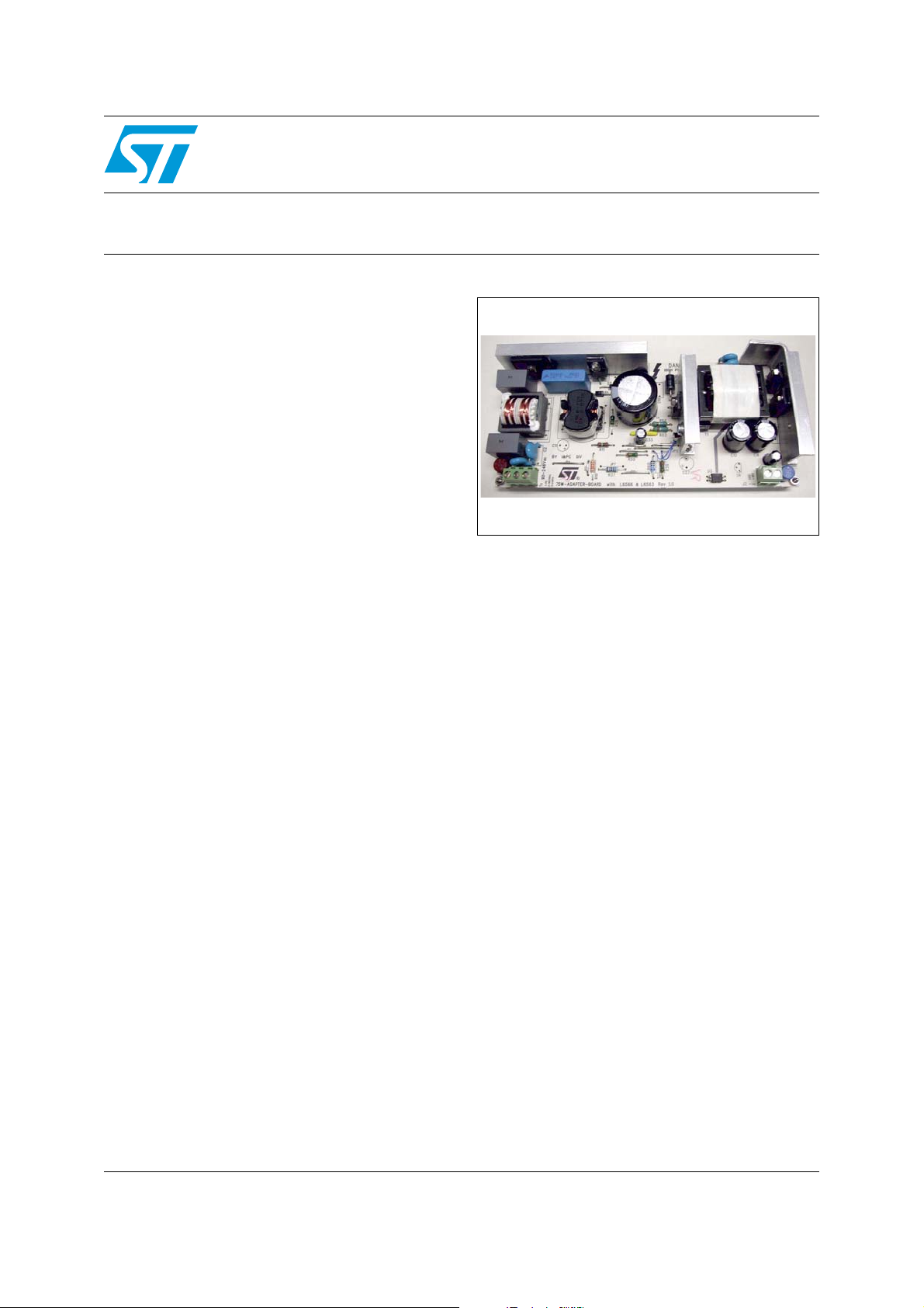
19 V - 75 W laptop adapter with tracking boost
PFC pre-regulator, using the L6563 and the L6566A
Features
■ Universal input mains range: 90÷264Vac -
Frequency 45 ÷ 65 Hz
■ Output voltage: 19 V@4 A continuous
operation
■ Mains harmonics: Acc. to EN61000-3-2
Class-D
■ ST-by mains consumption: Less than 0.25 W
@265Vac
■ Overall efficiency: Better than 86%
■ EMI: According to EN55022-Class-B
■ Safety: According to EN60950
■ Low profile design: 25 mm maximum height
■ PCB single layer: single side, 70 µm, CEM-1,
78x174 mm, Mixed PTH/SMT
EVL6566A-75WADP
Data Brief
Description
In this data brief of the EVL6566A-75WADP demo
board, the main characteristics and features of a
75 W adapter wide-range input mains, powerfactor-corrected AC-DC adapter using the new
L6566A controller and the L6563 dedicated to the
PFC stage are described.
High efficiency and the very low standby input
consumption are highlighted in the following
figures and tables. The board is programmed for
working at fixed frequency (65 kHz) under
nominal condition (19 V at 4 A).
On the secondary side the TSM1014 with a
precise voltage reference and the optocoupler
SFH617A-4 to transfer the error amplifiers
information to the primary side have been used.
September 2007 Rev 1 1/8
For further information contact your local STMicroelectronics sales office.
www.st.com
8
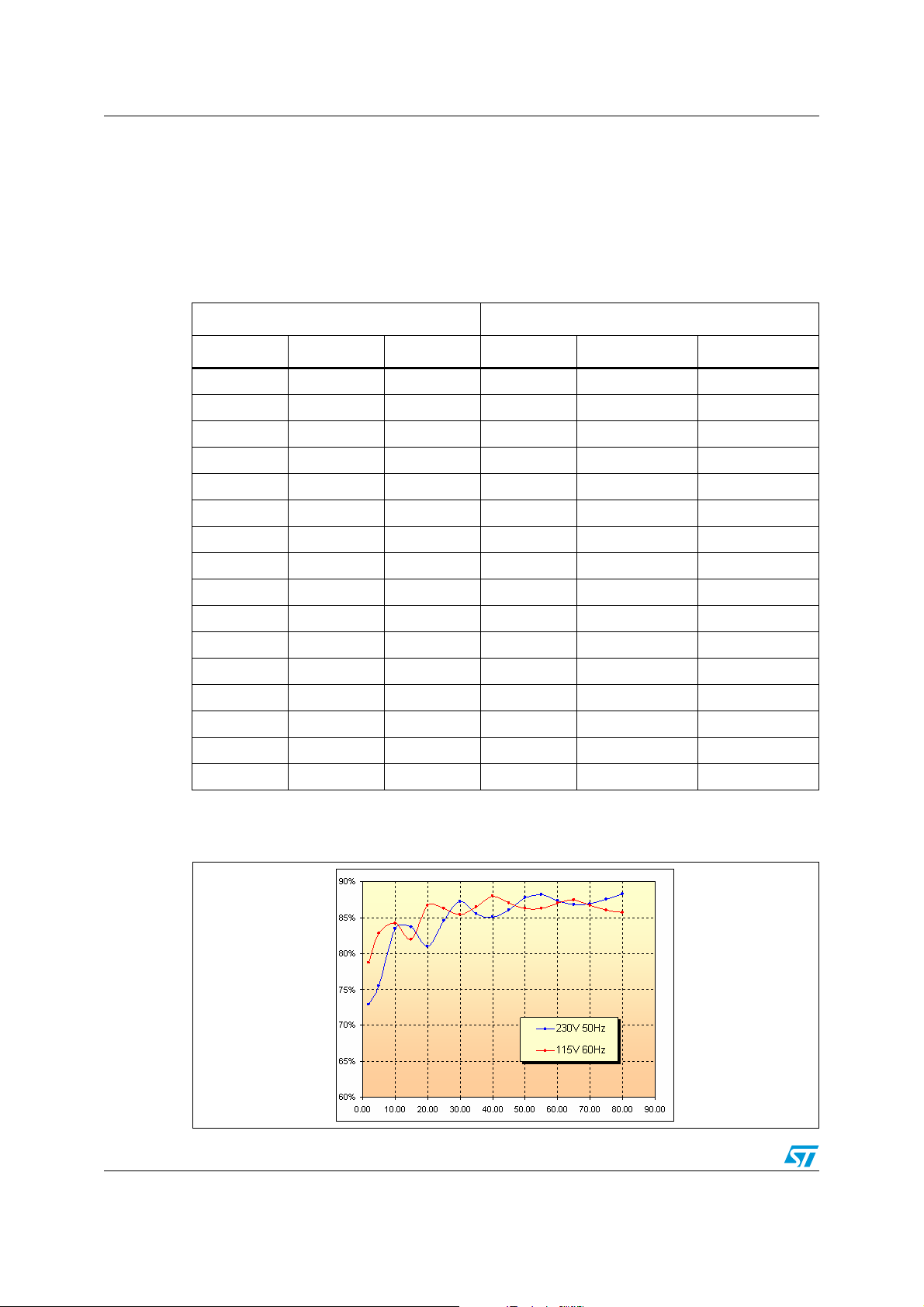
Efficiency EVL6566A-75WADP
1 Efficiency
Tab l e 1 below shows the efficiency with two different input voltages. The table begins with
the nominal load at 80 W on the output and it displays the efficiency at every power
decrease of 5 W.
Table 1. Efficiency measurements
230 V-50 Hz 115 V-60 Hz
Pin Pout Eff. Pin Pout Eff.
85.73 75.05 87.5% 87.24 75.06 86.0%
80.56 70.00 86.9% 80.73 70.00 86.7%
74.91 65.01 86.8% 74.34 65.01 87.4%
68.68 59.97 87.3% 68.95 60.00 87.0%
62.40 55.01 88.2% 63.80 55.02 86.2%
56.96 50.00 87.8% 58.03 50.04 86.2%
52.31 45.02 86.1% 51.80 45.05 87.0%
47.03 40.00 85.1% 45.45 40.00 88.0%
41.01 35.05 85.5% 40.53 35.05 86.5%
34.40 30.00 87.2% 35.15 30.00 85.3%
29.60 25.02 84.5% 29.00 25.02 86.3%
24.70 20.00 81.0% 23.07 20.00 86.7%
17.86 14.94 83.7% 18.36 15.05 82.0%
11.98 10.00 83.5% 11.88 10.00 84.2%
6.64 5.01 75.5% 6.10 5.05 82.8%
2.73 1.99 72.9% 2.53 1.99 78.7%
Above the 20 W power output, the efficiency is constant over 85%.
Figure 1. Overall efficiency versus output power at nominal mains voltages
2/8
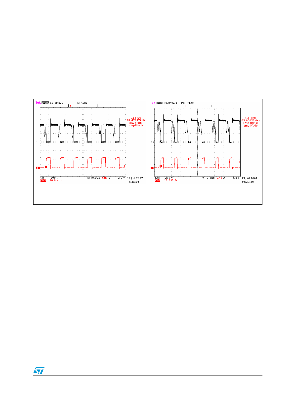
EVL6566A-75WADP Full load
2 Full load
Figure 2 and Figure 3 below show the drain and gate fly-back waveforms and the relevant
switching frequency at full load.
Figure 2. L6566A fly-back stage
waveforms at 115 V-60 Hz full load
CH1: drain 6566A
CH2: gate 6566A
Figure 3. L6566A fly-back stage
waveforms at 230 V-50 Hz full load
CH1: drain 6566A
CH2: gate 6566A
3/8

Light load condition (fold back frequency) EVL6566A-75WADP
3 Light load condition (fold back frequency)
To improve the efficiency at light load, a frequency shifting has been implemented on the
board. Thus, at decreasing load, the frequency also decreases. Figure 4 and Figure 5 below
show the drain and gate fly-back waveforms and the relevant switching frequency with a
load of 0.2 A.
Figure 4. L6566A fly-back stage
waveforms at 115 V-60 Hz 0.2 A
Figure 5. L6566A fly-back stage
waveforms at 230 V-50 Hz full load
CH1: drain 6566A
CH2: gate 6566A
Tab l e 2 below shows the efficiency when we set the power input with 2.4 or 1.7 W in two
different voltage inputs with the fold back network plugged in.
Table 2. Standby consumption
CH1: drain 6566A
CH2: gate 6566A
Light load condition
Vin = 230 V Vin = 115 V
Pin 2.401.692.411.71
Pout 1.51 1.06 1.70 1.14
Efficiency 62.9% 62.7% 70.5% 66.7%
4/8

EVL6566A-75WADP No-load
4 No-load
Tab l e 3 gives the power consumption of the circuit during no-load operation. Figure 6 and
Figure 7 show the main waveforms under this condition.
Table 3. No-load consumption
Vin [Vrms] Input power [W]
90 0.94
115 0.107
230 0.202
265 0.260
Figure 6. L6566A fly-back stage
waveforms at 115 V-60 Hz no-load
CH1: drain 6566A
CH2: V
CH3: V
6566A
cc
adapter
out
Figure 7. L6566A fly-back stage
waveforms at 230 V-50 Hz no-load
CH1: drain 6566A
CH2: V
CH3: V
6566A
cc
adapter
out
5/8

Schematic EVL6566A-75WADP
D1
5 Schematic
Figure 8. EVL6562A-TM-80W schematic
R55
22R
R55
22R
1
2
J2
19V@4A
MKDS 1,5/ 2-5,08J2MKDS 1,5/ 2-5,08
C17
100N
C17
100N
100u - 25V
100u - 25V
C13
C13
R22
R015
R22
L3
TSL0706 - 1R5-4R3
L3
TSL0706 - 1R5-4R3
R78
2K2
R78
2K2
R77
100K
R77
100K
D17
BZV55-B18
D17
BZV55-B18
R66
3R9
R66
3R9
D5
STPS20H100CFPD5STPS20H100CFP
R14
3R9
R14
3R9
C8
1N0C81N0
C7
2N2C72N2
R3
2M2R32M2
R2
680KR2680K
C6
100u - 450VC6100u - 450V
R1
NTC 10R-S236R1NTC 10R-S236
D3
STTH2L06D3STTH2L06
1N4005D11N4005
3
5
L2
L2
SRW25CQ-T05V102
SRW25CQ-T05V102
6
8
C5
470N - 400VC5470N - 400V
+
+
_
_
D2
D2
~
~
GBU4J
GBU4J
~
~
C4
470NC4470N
L1
HF2422-203Y1R0-T01
L1
HF2422-203Y1R0-T01
C2
2N2C22N2
C1
2N2C12N2
F1
FUSE 4AF1FUSE 4A
J1
123
MKDS 1,5/ 3-5,08J1MKDS 1,5/ 3-5,08
C3
470NC3470N
HS3
HEAT-SINK
HS3
HEAT-SINK
R11
2M2
R11
2M2
R5
2M2R52M2
R6
680KR6680K
R28
680K
R28
680K
R9
75KR975K
R8
75KR875K
Q2
R4
68KR468K
U1
L6563U1L6563
C9
100NC9100N
R7
3M3R73M3
R12
3M3
R12
3M3
100K
100K
R15
R15
R015
Q11
Q11
BC847C
BC847C
Q10
BC847C
Q10
BC847C
R75
1K8
R75
1K8
R76
4K7
R76
4K7
1000u - 25V
1000u - 25V
C16
C16
1000u - 25V
1000u - 25V
C12
C12
D7
STPS20H100CFPD7STPS20H100CFP
10-11
15-16
HS1
HS1
13
GD
62K
62K
1u
HEAT-SINK
HEAT-SINK
R23
27R
R23
27R
D8
12
R24
R24
GND
5-6
STTH108AD8STTH108A
100K
100K
C19
C19
R18
R18
8
R27
0R33
R27
0R33
11
9
10
ZCD
RUN
PWM-STOP
C21
470N
C21
470N
2N2
2N2
51K
51K
2-3
D4
1.5KE250AD41.5KE250A
STP9NK50ZFPQ2STP9NK50ZFP
C14
220N
C14
220N
14
VCC
INV1COMP2MULT3CS4VFF5TBO6PFC-OK
R17
R17
C151uC15
9
R25
R25
8
PWM-LATCH
7
C24
2N2
C24
2N2
T1
SRW32EC-T01H114
T1
SRW32EC-T01H114
HS2
HEAT-SINK
HS2
HEAT-SINK
Q5
STP10NK80ZFPQ5STP10NK80ZFP
R47
100K
R47
100K
R35
2R7
R35
2R7
R43
4R7
R43
4R7
R46
15R
R46
15R
D12
LL4148
D12
LL4148
D11
STTH102A
D11
STTH102A
D16
R37
10K
R37
10K
2N2
2N2
16
15
VFF
AC_OK
N.C.2GND3GD4VCC5VCC_PFC6DIS
HV
L6566AU6L6566A
1
R64
150K
R64
150K
C23
100N
C23
100N
D16
C34
C34
33K
33K
R42
R42
14
SS
R72
0R0
R72
0R0
C30
R10
33K
R10
33K
R19
3K0
R19
3K0
470R
470R
R33
0R0
R33
0R0
C26
22N
C26
22N
R30
22K
R30
22K
C25
220p
C25
220p
R34
390K
R34
R26
R26
390K
0R0
0R0
C30
U6
C33
47u - 50V
C33
47u - 50V
C32
100N
C32
100N
R62
100K
R62
100K
Q3
BC847CQ3BC847C
R50
1K0
R50
1K0
R69
1K0
R69
1K0
R67
12K
R67
12K
R36
1K8
R36
1K8
R32
15K
R32
15K
R31
39K
R31
39K
R53
0R56
R53
0R56
R52
0R56
R52
0R56
R51
1K0
R51
1K0
R60
6K8
R60
6K8
LL4148
LL4148
47N
47N
12
9
11
10
13
ZCD
OSC
VREF
COMP
MODE/SC
CS
8
7
R68
R68
R57
100R
R57
100R
C38
220p
C38
220p
8
VCC
U5
V_REF
1
220K
220K
R45
2K2
R45
2K2
12
43
U3
SFH617A-4U3SFH617A-4
R70
18K
R70
18K
C41
10N
C41
10N
R59
12K
R59
12K
OTP PROT
R58
M57703
R58
M57703
C40
C40
R63
100K
R63
100K
C36
100N
C36
100N
7
6
5
C43
2N2
C43
2N2
GND
CV_OUT
CC_OUT
TSM1014AISTU5TSM1014AIST
CV-
CC+3CC-
4
2
R65
22K
R65
22K
C441NC44
1N
R39
56K
R39
56K
R49
24K
R49
24K
R48
4K7
R48
4K7
C35
220N
C35
220N
R54
47K
R54
47K
R74
47K
R74
47K
Q9
BC857CQ9BC857C
C39
100N
C39
100N
10N
10N
90-264Vac
6/8

EVL6566A-75WADP Revision history
6 Revision history
Table 4. Document revision history
Date Revision Changes
28-Sep-2007 1 Initial release
7/8

EVL6566A-75WADP
Please Read Carefully:
Information in this document is provided solely in connection with ST products. STMicroelectronics NV and its subsidiaries (“ST”) reserve the
right to make changes, corrections, modifications or improvements, to this document, and the products and services described herein at any
time, without notice.
All ST products are sold pursuant to ST’s terms and conditions of sale.
Purchasers are solely responsible for the choice, selection and use of the ST products and services described herein, and ST assumes no
liability whatsoever relating to the choice, selection or use of the ST products and services described herein.
No license, express or implied, by estoppel or otherwise, to any intellectual property rights is granted under this document. If any part of this
document refers to any third party products or services it shall not be deemed a license grant by ST for the use of such third party products
or services, or any intellectual property contained therein or considered as a warranty covering the use in any manner whatsoever of such
third party products or services or any intellectual property contained therein.
UNLESS OTHERWISE SET FORTH IN ST’S TERMS AND CONDITIONS OF SALE ST DISCLAIMS ANY EXPRESS OR IMPLIED
WARRANTY WITH RESPECT TO THE USE AND/OR SALE OF ST PRODUCTS INCLUDING WITHOUT LIMITATION IMPLIED
WARRANTIES OF MERCHANTABILITY, FITNESS FOR A PARTICULAR PURPOSE (AND THEIR EQUIVALENTS UNDER THE LAWS
OF ANY JURISDICTION), OR INFRINGEMENT OF ANY PATENT, COPYRIGHT OR OTHER INTELLECTUAL PROPERTY RIGHT.
UNLESS EXPRESSLY APPROVED IN WRITING BY AN AUTHORIZED ST REPRESENTATIVE, ST PRODUCTS ARE NOT
RECOMMENDED, AUTHORIZED OR WARRANTED FOR USE IN MILITARY, AIR CRAFT, SPACE, LIFE SAVING, OR LIFE SUSTAINING
APPLICATIONS, NOR IN PRODUCTS OR SYSTEMS WHERE FAILURE OR MALFUNCTION MAY RESULT IN PERSONAL INJURY,
DEATH, OR SEVERE PROPERTY OR ENVIRONMENTAL DAMAGE. ST PRODUCTS WHICH ARE NOT SPECIFIED AS "AUTOMOTIVE
GRADE" MAY ONLY BE USED IN AUTOMOTIVE APPLICATIONS AT USER’S OWN RISK.
Resale of ST products with provisions different from the statements and/or technical features set forth in this document shall immediately void
any warranty granted by ST for the ST product or service described herein and shall not create or extend in any manner whatsoever, any
liability of ST.
ST and the ST logo are trademarks or registered trademarks of ST in various countries.
Information in this document supersedes and replaces all information previously supplied.
The ST logo is a registered trademark of STMicroelectronics. All other names are the property of their respective owners.
© 2007 STMicroelectronics - All rights reserved
STMicroelectronics group of companies
Australia - Belgium - Brazil - Canada - China - Czech Republic - Finland - France - Germany - Hong Kong - India - Israel - Italy - Japan -
Malaysia - Malta - Morocco - Singapore - Spain - Sweden - Switzerland - United Kingdom - United States of America
www.st.com
8/8
 Loading...