

Features
■ Input mains range:
– Vin: 88 ~ 264 Vrms
– Frequency: 45 ~ 66 Hz
■ Outputs:
– +12 Vdc ± 2% - 13.5 A
– +5 Vdc ± 2% - 12 A
– +3.3 Vdc ± 2% - 8 A
– +5 Vstby ± 2% - 2 A
■ Stand-by consumption: < 0.2 W
■ Protections:
– Short-circuit
–Overload
– Ouput overvoltage
– Brownout
■ PCB type and size:
–FR4
– Double side CU 70µm
– 148 x 120 mm
■ Safety: according to EN60950
■ EMI: according to EN55022 - class B
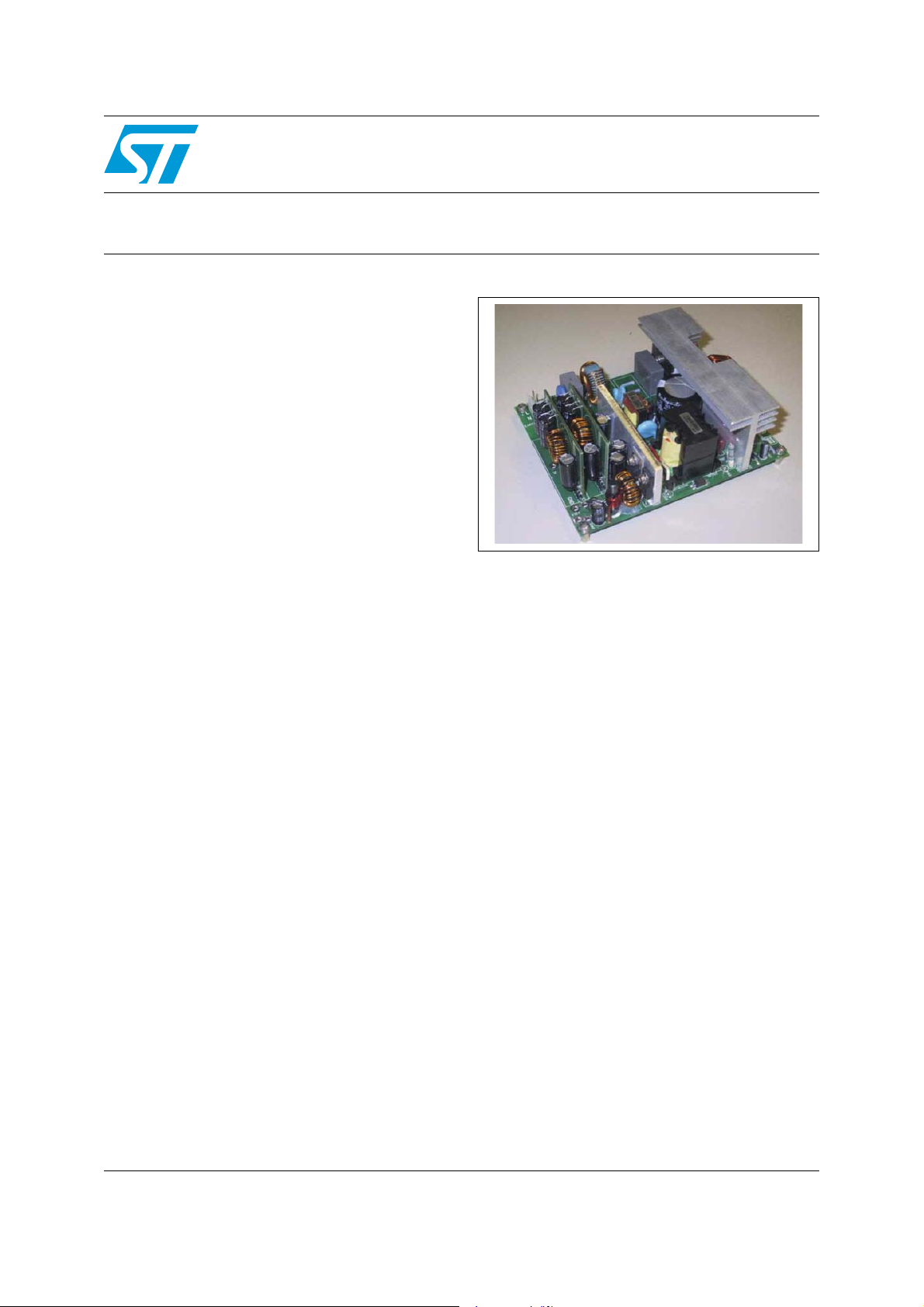
EVL250W-ATX80PL
250 W ATX SMPS demonstration board
Data brief
Description
The EVL250W-ATX80PL is a demonstration
board of a 250 W power supply unit that
implements an ATX like (multiple output
configuration) or a server like (single output
configuration) design.
The EVL250W-ATX80PL has been certified by
ECOS Consulting committee compliant to the 80
®
PLUS
specifications.
February 2011 Doc ID 010003 Rev 1 1/4
For further information contact your local STMicroelectronics sales office.
www.st.com
4

Instructions EVL250W-ATX80PL
1 Instructions
The converter consists of four main blocks:
● a PFC front-end stage using the L6563S PFC controller that generates the +400 V bus
voltage.
● an AHB (asymmetrical half bridge) stage using the L6591 ZVS half bridge controller
which performs the conversion from the high voltage bus to the +12 V output providing
insulation.
● two DC-DC post-regulator stages using the L6727 which obtain the +5 V and +3.3 V
outputs from the +12 V bus (for multiple output configuration).
● an auxiliary power supply (stand-by) stage using the VIPer27H in isolated flyback
configuration that provides the +5 V stand-by output with 10 W power capability.
The PFC stage is realized using a boost topology working in line modulated fixed off time
(LM-FOT) mode which offers the advantage of having CCM operation (with lower rms
current with respect to TM mode) without the needing to use a complex and expensive
controller.
The second stage is an asymmetrical half bridge converter, driven by the L6591, a
STMicroelectronics controller dedicated to this topology. This IC integrates all the functions
and protections needed by the AHB stage and an interface for the PFC controller. The
L6591 includes two gate drivers for the half bridge MOSFETs, a fixed frequency
complementary PWM logic with 50% maximum duty cycle with programmable dead time
and current mode control technique.
The last stage is the auxiliary power supply that provides the +5V stby output (2 A capability)
and the VCC supply for the L6563S and L6591. It is realized with a standard flyback
topology operating in CCM/DCM with fixed frequency using the VIPer27H. This stage takes
the PFC output voltage as input and it is always working when the mains is plugged. The
VIPer27H has all the protections to safely drive the stand-by stage.
The overall efficiency of the board is very high and it is given by the product of the efficiency
of each stage, in fact, the multiple output configuration is compliant with 80 PLUS
level of efficiency, according to 80 PLUS
®
initiative.
®
Silver
The single output configuration can be obtained from the complete system just removing the
two daughter boards that realize the DC-DC post regulation. This configuration can manage
the same power of the multi-output board achieving higher level of efficiency with respect to
the multiple output one, over performing 80 PLUS
®
Gold level of efficiency.
2/4 Doc ID 010003 Rev 1
 Loading...