

Page 1

Introduction
The EVALSP820-XS is an easy to use evaluation board for the STSPIN820, providing a compact solution to evaluate the
performance of the STSPIN820 stepper motor driver with minimal external equipment and without the need for extra
components.
The hardware is fully compatible with RepRAp Arduino Mega Poloulo Shield (RAMPS) or other similar Fused Filament
Fabrication (FFF) 3D Printing platforms, representing a very fast drop-in replacement of similar solutions. Contrary to most other
competitor solutions, the EVALSP820-XS helps customers to really exploit the benefits of working at high microstepping
resolution.
Getting started with the EVALSP820-XS evaluation board
UM2434
User manual
UM2434 - Rev 1 - June 2018
For further information contact your local STMicroelectronics sales office.
www.st.com
Page 2
1 Board overview
The main characteristics of the board are:
• Supply voltage from 7 V to 45 V
• Output current up to 1.5 A rms for each motor phase
• Peak current regulation through trimmer
• Form factor and connectivity compatible with RAMPS (RepRap Arduino Mega Pololu Shield) or similar
boards
• Based on STSPIN820 driver featuring:
–
Stepper motor driving with a microstepping resolution up to 1/256th of step
– Overcurrent, short-circuit and overtemperature protections
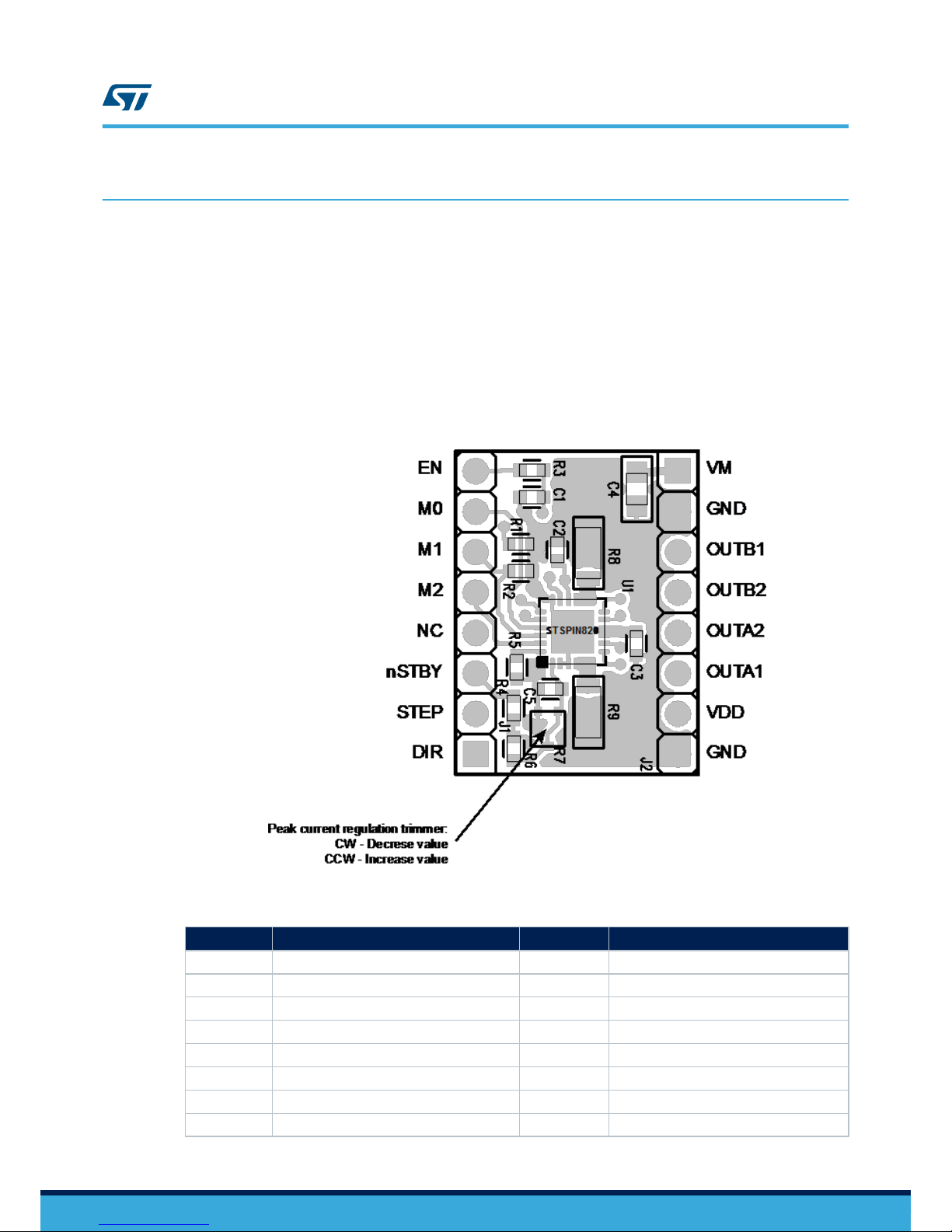
Figure 1. Board overview
Table 1. Board pinout
J1
Signal J2 Signal
8 Enable (EN) 1 Motor supply voltage (VM)
7 Step mode selection input (M0) 2 Ground
6 Step mode selection input (M1) 3 Phase B out 1 (OUTB1)
5 Step mode selection input (M2) 4 Phase B out 2 (OUTB2)
4 NC 5 Phase A out 2 (OUTA2)
3 Active low standby (nSTBY) 6 Phase A out 1 (OUTA1)
2 Step-clock input (STEP) 7 Logic supply voltage (VDD)
1 Direction input (DIR) 8 Ground
UM2434
Board overview
UM2434 - Rev 1
page 2/11
Page 3
2 Quick start
2.1 Safety precautions
Note: Warning! Some of the components mounted on the board could reach hazardous temperatures during
operation.
While using the board, please adhere to the following precautions
• Do not touch the components
• Do not cover the board
• Do not put the board in contact with flammable materials of with materials releasing smoke when heated
After operation, allow the board to cool down before touching it.
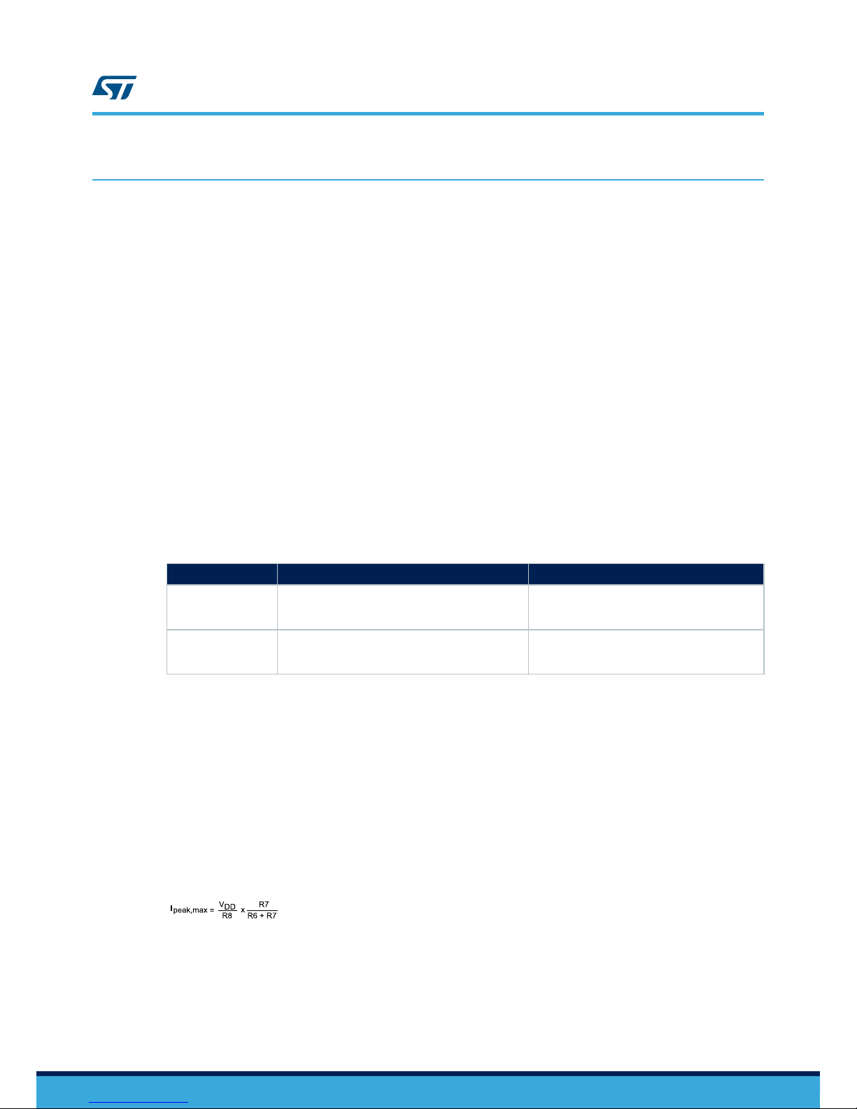
2.2 Adjusting motor peak current
The R7 trimmer adjusts the reference voltage of the STSPIN820 PWM current controller setting the peak current
input to the motor phases.
The R7 trimmer controls the current level. Rotating clockwise increases and rotating counter clockwise decrease
the current level.
The range depends on the VDD logic supply voltage (pin 6 of J2) as listed in the table below.
Table 2. Peak current ranges
VDD Minimum Maximum
3.3 V V
REF
= 0 V
I
peak
= 0 A
(1)
V
REF
= 0.67 V
I
peak
= 4.5 A
(2)
5 V V
REF
= 0 V
I
peak
= 0 A
(1)
V
REF
= 1 V
I
peak
= 6.8 A
(2)
(1)
Minimum current could be present due to the PWM current control operation
(2)
The overcurrent protection of the STSPIN820 could limit the actual peak current
2.2.1 Modify the peak current range
The trimmer can be adjusted by modifying some board components.
In particular the components contributing to the definition of the peak current are:
• Both the sensing resistors
• Pull-up resistor (R6)
• Sensing resistor (R8 and R9)
The detailed formula is the following:
Changing the sensing resistors requires particular attention:
• Bust the sensing resistors must have the same value
•
Power dissipation on the resistors is equal to I
peak
2
× R
sense
. The power rating must be selected accordingly.
UM2434
Quick start
UM2434 - Rev 1
page 3/11
Page 4
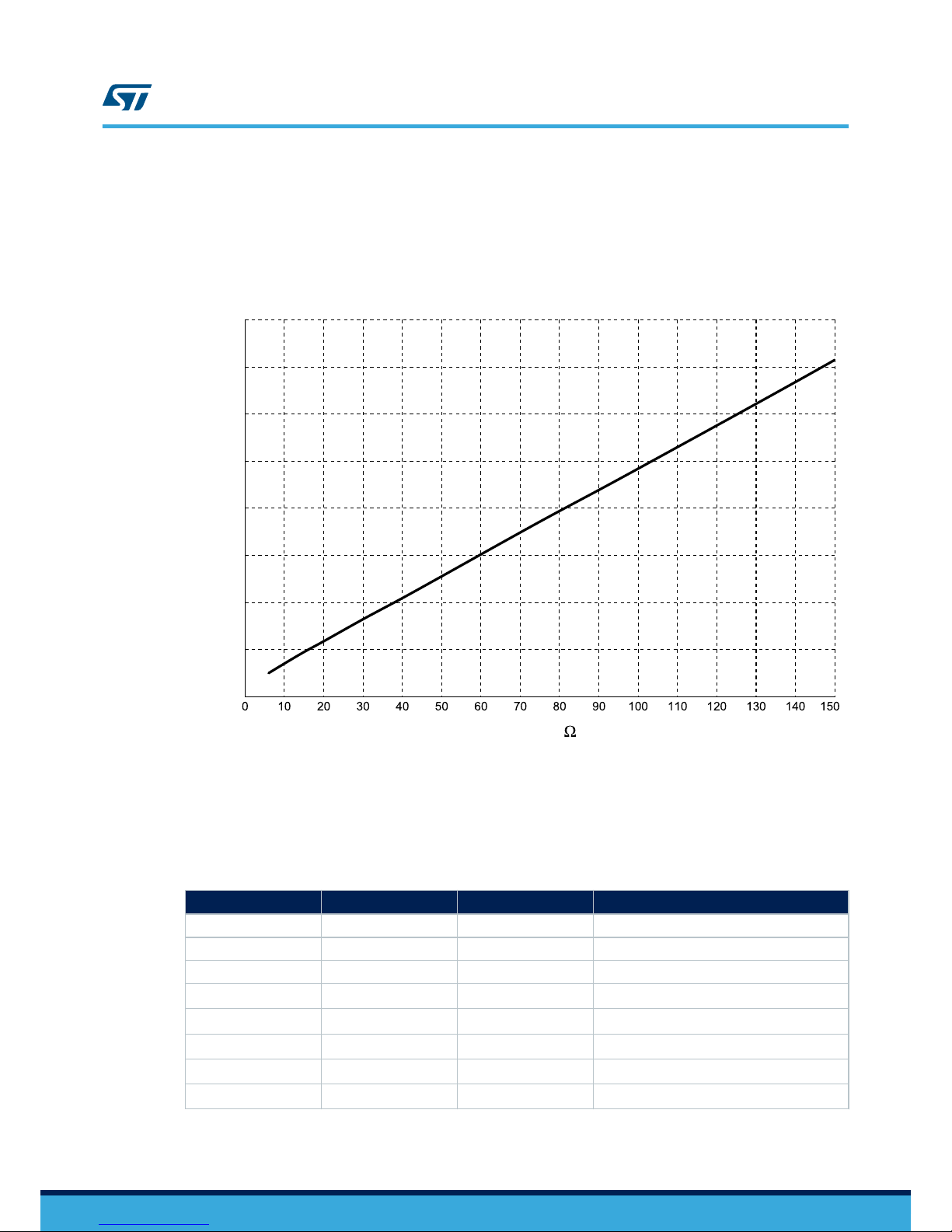
2.3 Setting off time duration
The R5 resistor sets the off time duration for the PWM current control circuitry as indicated in the figure below.
Low resistance value imposes a short off time reducing the current ripple into the motor phases.
The default value is 10 kΩ, corresponding to about 14 µs.
Figure 2. OFF time vs R
OFF
value
0
20
40
60
80
100
120
140
160
OFF time [µs ]
R
OFF
[k ]
AM040213
2.4
Setting the step mode
The inputs M0, M1 and M2 sets the step mode of the STSPIN820 driver as listed in the table below.
Table 3. Step mode selection
M2 M1 M0 Mode
LOW LOW LOW Full step
LOW LOW HIGH ½ step
LOW HIGH LOW ¼ of step
LOW HIGH HIGH
1/8th of step
HIGH LOW LOW
1/16
th
of step
HIGH LOW HIGH
1/32
nd
of step
HIGH HIGH 0
1/128
th
of step
HIGH HIGH HIGH
1/256
th
of step
UM2434
Setting off time duration
UM2434 - Rev 1
page 4/11
Page 5

3 Schematic, layout and bill of material
Figure 3. Schematic
VDD
VMOT
B1
B2
A2
A1
GND
GND
Connected on
RAMP 1.4
VCC
VCC
VCC
C1
10NF
C5
1NF
U1
STSPIN820
STBY/RESET
16
EN/FAULT
17
DIR
20
STCK
19
MODE3
23
MODE1
21
REF
1
TOFF
24
VS
9
OUTA1
7
OUTA2
8
SENSEA1
5
OUTB1
12
OUTB2
11
SENSEB1
14
GND2EPAD
25
DECAY
18
MODE2
22
VS
10
SENSEA2
6
SENSEB2
13
SNSA
4
SNSB
15
GND
3
R9
0.15R
R7
10K
ST2TA103
1 3
2
R8
0.15R
C2
1NF
R2
100K
C4
4.7UF
50V
R3 39K
J2
1
2
3
4
5
6
7
8
R6
39K
R4
18K
J1
1
2
3
4
5
6
7
8
R5
10K
R1
100K
C3
100NF
OUTB1
OUTB2
DIR
M2
M1
M0
EN
VMM
STEP
OUTA1
OUTA2
AM040394
Figure 4. Layout top
AM040395
Figure 5. Layout bottom
AM040396
UM2434
Schematic, layout and bill of material
UM2434 - Rev 1
page 5/11
Page 6

Table 4. Bill of material
Item Qty. Ref. Part/ value Voltage/ watt/
ampere
Tolerance Package Manufacturer Orderable part
number
1 1 C1 10 NF 50 V 0.15 0603
2 2 C2, C5 1 NF 50 V 0.15 0603
3 1 C3 100 NF 100 V 0.15 0603
4 1 C4 4.7 UF 50 V 0.15 0805
5 2 J1, J2 61300811121 WURTH
ELECTRONIK
61300811121
6 2 R1, R2 100 K 1/10 W 0.05 0603
7 2 R3, R6 39 K 1/10 W 0.05 0603
8 1 R4 18 K 1/10 W 0.05 0603
9 1 R5 10 K 1/10 W 0.05 0603
10 1 R7 10 K 1/10 W 0.2 L2.75_W2.2_H0.8 BOURNS TC42X-2-103
11 2 R8, R9 0.15 R 1/2 W 0.01 1206
12 1 U1 STSPIN820 QFN24_L4_W4_P0.5 ST STSPIN820
UM2434
Schematic, layout and bill of material
UM2434 - Rev 1
page 6/11
Page 7

Revision history
Table 5. Document revision history
Date Version Changes
28-Jun-2018 1 Initial release.
UM2434
UM2434 - Rev 1
page 7/11
Page 8

Contents
1 Board overview ...................................................................2
2 Quick start ........................................................................3
2.1 Safety precautions .............................................................3
2.2 Adjusting motor peak current.....................................................3
2.2.1 Modify the peak current range...............................................3
2.3 Setting off time duration .........................................................3
2.4 Setting the step mode...........................................................4
3 Schematic, layout and bill of material ..............................................5
Revision history ........................................................................7
UM2434
Contents
UM2434 - Rev 1
page 8/11
Page 9

List of tables
Table 1. Board pinout .......................................................................2
Table 2. Peak current ranges.................................................................. 3
Table 3. Step mode selection..................................................................4
Table 4. Bill of material ......................................................................6
Table 5. Document revision history..............................................................7
UM2434
List of tables
UM2434 - Rev 1
page 9/11
Page 10

List of figures
Figure 1. Board overview....................................................................2
Figure 2. OFF time vs R
OFF
value .............................................................4
Figure 3. Schematic .......................................................................5
Figure 4. Layout top .......................................................................5
Figure 5. Layout bottom ....................................................................5
UM2434
List of figures
UM2434 - Rev 1
page 10/11
Page 11

IMPORTANT NOTICE – PLEASE READ CAREFULLY
STMicroelectronics NV and its subsidiaries (“ST”) reserve the right to make changes, corrections, enhancements, modifications, and improvements to ST
products and/or to this document at any time without notice. Purchasers should obtain the latest relevant information on ST products before placing orders. ST
products are sold pursuant to ST’s terms and conditions of sale in place at the time of order acknowledgement.
Purchasers are solely responsible for the choice, selection, and use of ST products and ST assumes no liability for application assistance or the design of
Purchasers’ products.
No license, express or implied, to any intellectual property right is granted by ST herein.
Resale of ST products with provisions different from the information set forth herein shall void any warranty granted by ST for such product.
ST and the ST logo are trademarks of ST. All other product or service names are the property of their respective owners.
Information in this document supersedes and replaces information previously supplied in any prior versions of this document.
© 2018 STMicroelectronics – All rights reserved
UM2434
UM2434 - Rev 1
page 11/11
 Loading...