

Page 1

UM2605
User manual
EVAL-RHRICL1ATV1, EVAL-RHRICL1ALV1, EVAL-RHRICL1AFV1 evaluation
boards for the RHRPMICL1A
Introduction
This user manual provides an overview of the EVAL-RHRICL1ATV1, EVAL-RHRICL1ALV1 and EVAL-RHRICL1AFV1 evaluation
boards developed for the RHRPMICL1A, rad-hard integrated current limiter IC. One evaluation board for each of the three
operative modes of the RHRPMICL1A is available. Each evaluation tool includes all external components, needed for a
complete electrical evaluation of the device functionality in the selected configuration.
Table 1. Application tools
Type Part number Configuration Marking
Evaluation tools EVAL-RHRICL1ATV1 Re-triggerable RHRPMICL1ATV1 -RE-TRIGGERABLE
Evaluation tools EVAL-RHRICL1ALV1 Latched RHRPMICL1ALV1 - LATCHED ON/OFF
Evaluation tools EVAL-RHRICL1AFV1 Foldback RHRPMICL1AFV1 --FOLDBACK
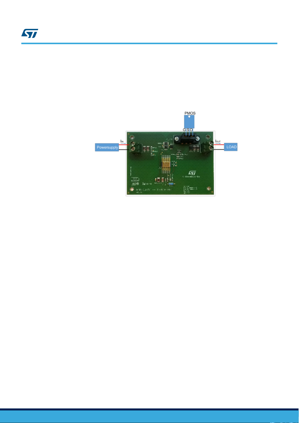
Figure 1. EVAL-RHRICL1ATV1 (re-triggerable)
Figure 3. EVAL-RHRICL1AFV1 (foldback evaluation board)
Figure 2. EVAL-RHRICL1ALV1 (latched evaluation board)
UM2605 - Rev 1 - July 2019
For further information contact your local STMicroelectronics sales office.
www.st.com
Page 2
1 Description
The RHRPMICL1A is an integrated current limiter designed to work as a high-side gate driver or intelligent power
switch driver, with an external P-channel power MOSFET. It can be used as a universal solution to protect a
power supply (from 8.5 V) from anomalous external current demand (for example, even in case of a short-circuit
condition).
The device can operate with a supply voltage range from 8.5 V to 52 V. An undervoltage lockout circuitry
guarantees the appropriate power supply integrity.
As the device can operate in floating ground configuration, in this user manual GND, the ground pin of the
RHRPMICL1A device (pin 7), and MGND the ground of main bus are defined.
In case of overload, the device behavior changes according to its configured mode of operation:
• Latched mode, the device provides current limitation capability for an external configurable time, called tripoff time, and if the overcurrent condition exceeds this time, the device switches OFF. In this case, the device
may be switched ON again through the telecommand pin only or a UVLO deactivation/activation cycle
• Re-triggerable mode, after the trip-off time, that is externally configurable, the device switches OFF and
remains in this state for a recovery time that is externally configurable. Once this time elapses, the device
recovers its typical operation mode if the overload condition disappears, otherwise it switches cyclically ON
and OFF again while the overload persists (hic-up mode)
• Foldback mode, in case of overload, the device provides current limitation with a value decreasing in
tracking with the output voltage, reaching a fixed and safe value even if a short-circuit persists
The mode of operation can be selected by configuring the RHRPMICL1A pins according to the following
configuration table, which is implemented in the evaluation boards:
UM2605
Description
Table 2. Applicable tools
Mode SET_FLB SET_STS TC_ON TC_OFF TON TOFF
Latched OFF 0 0 Telecommand Telecommand
Latched ON 0 1 Telecommand Telecommand
Re-triggerable 0 1 Vcc Vcc
Foldback 1 1 Vcc Vcc
1. GND refers to the RHRPMICL1A GND pin (pin 7), not to the main system ground (MGND).
C
C
C
GND
ON
ON
ON
(1)
GND
GND
C
OFF
GND
(1)
(1)
(1)
Status at
power-up
OFF
The characteristics and the main functionalities of each demonstration board are described in the following
sections.
ON
ON
ON
UM2605 - Rev 1
page 2/27
Page 3

2 Common features and parameters
This section describes the features that are in common to the three boards, such as: UVLO, floating ground
configuration, current limitation, analog and digital telemetries, and explains how to customize them by changing
the external components on the board.
2.1 Undervoltage lockout and hysteresis settings
UM2605
Common features and parameters
The UVLO and hysteresis can be programmed by a set of three resistors: the R
A 220 kΩ resistor is generally used for RV, the other two resistors are obtained by the following equations:
Where K=150 is a corrective fixed value to be added to Eq. (1) in order to take into account that during the rising
phase of supply voltage, in the UVLO external resistor divider, R
the RHRPMICL1A.
2.2 Gate driving
The driver circuit is designed to drive an external P-channel power MOSFET (connected in high-side
configuration) providing on the Vg pin a voltage signal in the range VCC down to (VCC - 12 V). All the evaluation
boards are equipped with a through-hole socket where the power MOSFET can be easily housed.
When the device is ON and no current limitation is active, the Vg node is pulled down and the gate of the external
MOSFET is internally clamped, about 12 V below the supply voltage VCC. When the MOSFET has to be switched
OFF, Vg is brought up to VCC.
When the MOSFET is in current limitation mode, the Vg voltage is a value inside the range [VCC-12 V, VCC],
defined by the limitation control loop.
2.3
Current sense and limitation function
The voltage drop on the external R
compared with a fixed 100 mV internally generated threshold.
The current limitation threshold can be externally set according to the application requirements by a suitable
choice of the R
In the re-triggerable and latched evaluation boards it is:
If the voltage drop on R
internal timer starts counting the trip-off time TON and the device enters the current limitation mode. In such a
condition the limitation control loop is enabled in order to force Vg to the proper voltage level, limiting the current
to the load.
Please refer Section 5.1.2.2 Bill of material of the EVAL-RHRICL1AFV1 board for the current limitation settings
in the foldback mode evaluation board.
SENSE
resistor.
SENSE
, R
HYS
2.5*R
R
=
UVLO
R
UVLO
resistor is continuously monitored (by ISNS+ and ISNS- pins) and
SENSE
I
LIM
=
V
V
TH_OFF
= 100mV/R
TH_ON
2.5*R
V
− 2.5
V
− 2.5
− R
SENSE
− K
UVLO
is shorted by a non-ideal switch embedded in
HYS
UVLO
and RV.
exceeds 100 mV means that the current demand is becoming excessive: an
(1)
(2)
(3)
2.4 Floating ground configuration
The evaluation boards are equipped with the R
(GND) and the system ground (MGND).
An embedded 14.8 V Zener diode chain allows the device to operate in floating ground configuration and protects
the ICL device as its internal voltage supply is clamped at VZ ~ 15 V (14.8 V typ).
According to the voltage value of the Bus supply and depending on the value of RGND, the device can work (or
not) in floating ground condition, as follows:
UM2605 - Rev 1
floating resistance mounted between the GND pin of the ICL
GND
page 3/27
Page 4
UM2605
Analog telemetry
1. Vcc <14.8 V
The Zener diode chain is OFF and the R
the device. Since the typical current consumption of the ICL device is ~ 1.5 mA (the current contribution of the
Zener diode chain is null in this case), in order to have a certain V
1. Vcc > 14.8 V
In this case the Zener diode chain is enabled and the R
consumption of the device, flowing through R
This current consumption is given by the sum of two contributors:
1. The net current consumption of the RHRPMICL1A (considering the internal Zener diode chain current as
zero)
2. The current consumption of the Zener diode chain in ON-state
For example, if we want to set the maximum current consumption of the RHRPMICL1A device to 2 mA, the value
of R
GND
is:
The RHRPMICL1A can be configured to work also with power Buses with voltage higher than 52 V, by adding the
proper protection components to the application.
Guidelines on this feature are provided in the RHRPMICL1A datasheet.
is used to protect the system against a potential internal failure of
GND
, the R
GND
V
R
GND
resistor from GND pin to the system ground MGND.
GND
R
GND
GND
=
1.5mA
GND
VCC− 14.8V
=
2mA
is also used to limite the maximum current
GND
value is:
(4)
(5)
2.5 Analog telemetry
The analog telemetry circuit gives information about the current flowing across the load. This circuit provides on
the TM pin a source current whose value is instantly proportional to the current flowing from the bus supply line to
the load. The voltage drop (VTM) on the external resistor RTM connected between the TM pin and MGND, is
proportional to the load current (I
) flowing through R
SENSE
RTM=
V
I
RTM
2.6 Digital telemetry (status telemetry)
The status telemetry circuit gives some information about the device status, which can be retrieved by monitoring
the STS output pin, according to the following table.
Table 3. Signal on digital telemetry pin
STS pin signal RHRPMICL1A driver status
HIGH ON
LOW OFF
The STS is an open drain pin that can source a 100 μA fixed current; it is typically connected to MGND through
an external resistor R
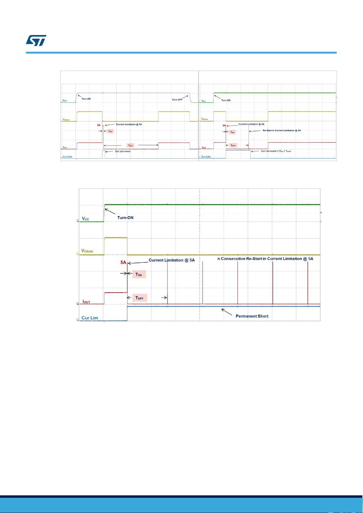
The following picture shows the telemetry signals during the ICL operation.
, setting the desired high logic level value V
STS
TM
=
V
TM
I
SENSE
, thus performing a current/voltage conversion:
SENSE
R
TMS
*
R
SENSE
as follows:
H_STS
(6)
UM2605 - Rev 1
page 4/27
Page 5
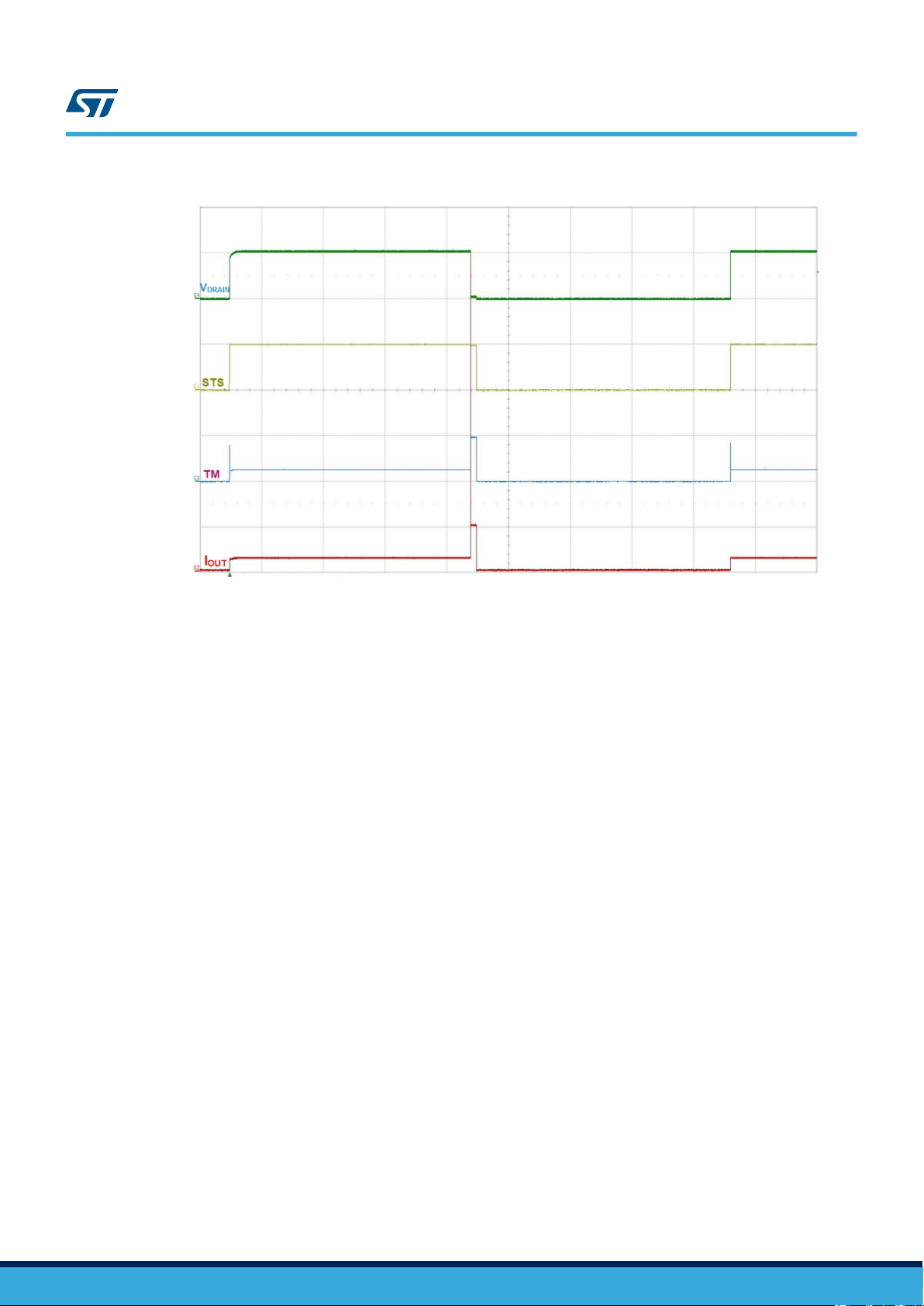
Figure 4. Telemetry signals
UM2605
Digital telemetry (status telemetry)
UM2605 - Rev 1
page 5/27
Page 6
CVcc_2_btm
4.7 uF
SCH2
STPS3150
Csts_2
4.7 pF
Ctm_2 4.7 pF
Csns_2 1uF
Rcomp_2
1k
C6
4.7uF
C8
4.7uF
ZD2
1SMB5929BT3G
U2
1
2345678
9
10
11
1718192016
15
14
13
12
VD_2
VCC+_2
P-ch2
STRH40P10
0
C5
4.7uF
Rhys_2
1.5k
Ruvlo_2
13k
Rv_2
220k
Rsns1_2
40m
VCC+_2
1
2
1
2
C7
4.7uF
0
Rsns2_2
40m
Rir_2
100k
RGND_2
16.2k
Con_2
27nF
I_STM- _1
I_STM+_1
Rtms+_2
5k
Rtms-_2
5k
ISNS
-_1
ISNS+_1
VCC+_2
VCC-_2
VCC-_2
Ccomp_2
2.2 nF
COMP_2
VD_2
CVcc_2
100nF
RETRIGGERABLE MODE
VCC+_2
SET_FLB
SET_STS
I_REF
T_ON
T_OFF
STS
ICL_GND
Rsts_2
50k
Rtm_2 100k
TM
0
HYS
UVLO
UVLO
HYS
VCC
Rg_2
4R7
Coff_2
470nF
TC_OFF
TC_ON
CN3
CN4
VG
CFLAT20
Features: EVAL-RHRICL1ATV1, re-triggerable mode
3 Features: EVAL-RHRICL1ATV1, re-triggerable mode
3.1 Getting started
The EVAL-RHRICL1ATV1 evaluation board is customized to allow the test of re-triggerable operative mode of the
RHRPMICL1A integrated current limiter (ICL).
In the re-triggerable mode, the ICL restarts automatically, recovering its normal operating mode if the current
limitation cause is removed; besides, during any overload or output short-condition events, after the T
recovery time elapses, the device tries to re-start for a dedicated TON slot time (trip-off time).
The configuration pins of the ICL in this mode are:
• Telecommand interface: disabled (TC_ON and TC_OFF both connected to VCC)
• SET_STS is connected to V
• SET_FLB is connected to GND
• TON is connected to C
• TON is connected to C
The external components of the board are pre-set to accomplish the following features:
• VCC = 50 V with V
TH_ON
• HYS = 4 V
• I
LIM
= 5 A
• TON ˜ 3 ms (typ 2.7 ms) with T
The evaluation board schematic is shown below. Please note that the capacitor Csns_2, connected in parallel to
the R
, affects the dynamic of the reaction time and therefore the decision whether to mount it or not is up to
SENSE
the application needs of the end user.
CC
ON
OFF
= 44 V and V
OFF
= 40 V
TH_OFF
˜ 1s (typ. 0.94 s)
UM2605
OFF
Figure 5. Re-triggerable evaluation board (schematic)
UM2605 - Rev 1
page 6/27
Page 7
3.2 Operations
3.2.1 Power-on and testing environment
Connect a 50 V power supply to CN3, the load on CN4. The telecommand section is not activated in this
evaluation board. The analog and digital telemetries are accessible on the RTM and R
Figure 6. Testing environment
resistors respectively.
STS
UM2605
Operations
3.2.2 Trip-on and trip-off time programming
In re-triggerable mode, if the duration of the overcurrent is greater than the trip-off time TON, the external
MOSFET is switched OFF after the TON time has elapsed and stays OFF for the recovery time T
T
time elapses, the device restarts autonomously to its normal condition, turning on again the MOSFET, if the
OFF
current limitation cause is removed. Otherwise it switches cyclically on and off again while the overload persists
(hic-up mode).
The trip-off time TON is set by the CON capacitor connected between the pins TON and GND, and it is calculated
by the following equation:
In the same way, the recovery time T
T
and GND. The C
OFF
capacitor is charged with a constant current whose value is a fraction (typ. 1/20) of I
OFF
current (externally set by the resistor RIR connected between the I_REF pin and GND). The charging phase of
C
capacitor starts as soon as the TON time has elapsed, therefore the T
OFF
time defined by:
In the equations above, unit for TON and T
The typical behavior of the device configured in re-triggerable mode is depicted below (timing is not in scale).
is set through the external capacitor C
OFF
OFF
. When the
OFF
TON= RIR*C
T
= 20*RIR*C
OFF
ON
OFF
connected between the pins
OFF
time is equal to the C
OFF
OFF
charging
are in seconds, for resistance in Ω and for capacitance in Farads.
(7)
REF
(8)
UM2605 - Rev 1
page 7/27
Page 8
UM2605
Operations
Figure 7. Overload shorter than TON+T
Figure 9. Continuous short-circuit
OFF
Figure 8. Overload longer than TON+T
OFF
UM2605 - Rev 1
page 8/27
Page 9
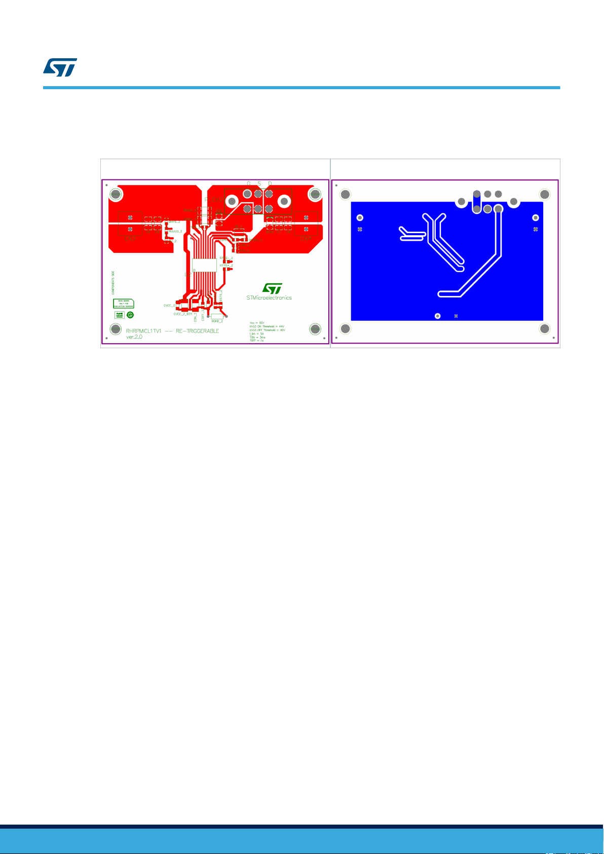
3.3.1 Layout of the EVAL-RHRICL1ATV1 board
UM2605
Operations
Figure 10. EVAL-RHRICL1ATV1 top layout
Figure 11. EVAL-RHRICL1ATV1 bottom layout
UM2605 - Rev 1
page 9/27
Page 10

3.3.2 Bill of material of the EVAL-RHRICL1ATV1 board
Table 4. Bill of material
UM2605
Operations
Item Qty Reference Part / value
1 2 CN3, CN4
2 4 C5,C6,C7,C8
3 1 CVcc_2_btm
4 1 CVcc_2 100 nF 100 V 1206 MULTICOMP MCCA000490 X7R 1206
5 1 Csns_2 1 μF 10 V 0805 KEMET
6 1 Coff_2 470 nF 50 V 0805 KEMET
7 1 Ccomp_2 2.2 nF 50 V 0805 AVX
8 2
9 1 Con_2 27 nF 50 V 1812 KEMET
10 1 Rv_2 220 kΩ
11 2
12 1 Rtm_2 100 kΩ
13 1 Rsts_2 50 kΩ
14 1
15 1 Rg_2 4.7 Ω 200 V, 1% 1 W Panasonic ERJB1BF4R7U 1020
16 2
17 1 Rhys_2 1.5 kΩ
18 1 Ruvlo_2 13 kΩ
19 1 Rcomp_2 1 kΩ
20 1 Rir_2 100 kΩ
21 1 ZD2 ZENER 15 V, 3 W
C_TM_2
C_STS_2
Rtms+_2,
Rtms-_2
RGND_2
(R_floating)
Rsns1_2
Rsns2_2
2PIN screw
connector
4.7 μF
capacitor
4.7 μF
capacitor
47 pF 50 V 0805 KEMET
5 kΩ
16.2 kΩ 1% 0.6 W Vishay
40 mΩ
Voltage
current
Pitch-6.35 mm TH
100 V 1812 TDK
100 V 1812 TDK
100 V, 0.1%,
25 ppm/°C
100 V, 0.1%, 5
ppm/°C
100 V, 0.1%,
25 ppm/°C
100 V, 0.1%,
25 ppm/°C
1%, 75 ppm/
100 V, 0.1%,
25 ppm/°C
100 V, 0.1%,
25 ppm/°C
0.1%, 25
ppm/°C
150 V, 0.1%,
25 ppm/°C
Package Manufacturer
0.125 W Panasonic ERA6AEB224V 0805
0.200 W Vishay thin film
0.125 W Panasonic ERA6AEB104V I=20 μA 0805
0.200 W Vishay
°C
1 W VISHAY
0.125 W Panasonic ERA6AEB152V 0805
0.125 W Panasonic ERA6AEB133V 0805
125 mW Panasonic ERA6AEB102V 0805
0.250 W Panasonic ERA8AEB104V I=10 μA 1206
Phoenix
contact
ON
SEMICONDUC
TORS
Manufacturer
code
1714955
C4532X7S2A475
M
C4532X7S2A475
M
C0805C105K8N
ACTU
C0805C474K5R
AC
08055C222JAT2
A
C0805C470J5G
ACTU
C1812C273J5G
ACTU
PNM0805E5001
BST5
PNM0805E5002
BST5
MBB02070C162
2FCT00
WSL2512R0400
FEA
1SMB5929BT3G Zener
More info Footprint
INPUT
(CN1) and
OUTPUT
(CN2)
connectors
X7S 1812
X7S 1812
X8L 0805
X7R 0805
X7R 0805
NPO 0805
NPO 1812
0805
I=100 μA 0805
I=0.5 A - 10
A
2512
SMB-
CASE403A
TH
UM2605 - Rev 1
page 10/27
Page 11

UM2605
Operations
Item Qty Reference Part / value
Voltage
current
Package Manufacturer
22 1 SCH2 STPS3150 3 A, 150 V ST STPS3150U
P-ch
23 1
P_ch2
SOCKET
TO254AA
socket
(for the
34 A, 100 V
3M TOUCH
SYSTEMS
STRH40P10)
Manufacturer
code
203-2737-55-110
2
More info Footprint
Diode 100
V-5 A
SMB
P-channel,
B
100 V,
Vdss
id 48 A,
R
DS(on)
60
TO-254 AA
mΩ, Qg 162
nC
24 1 U2 ICL001 FLAT20 ST FLAT20
UM2605 - Rev 1
page 11/27
Page 12

U1
CFLAT20
1
2345678
9
10 11
171819
20
16
151413
12
VD_1
TC_ON
P-ch1
STRH40P10
0
C1
4.7uF
Rv_1
220k
Rsns_1
50m
VCC+_1
CN1
1
2
CN2
1
2
C3
4.7uF
0
CVcc_1_btm
4.7 uF
Rir_1
100k
RGND_1
8.25k
Con_1
100 nF
I_STM+_1
I_STM- _1
Rtms+_1
5k
Rtms-_1
5k
ISNS+_1
ISNS
-
_1
VCC-_1
VCC+_1
VCC-_1
Ccomp_1
2.2 nF
LATCHING MODE
COMP_1
VD_1
1
3
SW1
2
CVcc_1
100nF
VCC+_1
LATCHED ON
LATCHED OFF
SET_FLB
SET_STS
TC_OFF
I_REF
T_ON
T_OFF
STS
ICL_GND
Rsts_1
50k
TM
Rtm_1 100k
0
UVLO
VG
HYS
HYS
UVLO
VCC
Rg_1
4R7
Csts_1
4.7 pF
Rtc_on_1
50K
Rtc_off_1
50K
SCH1STPS3150
Rcomp_1
1k
Ctm_1 4.7 pF
C2
4.7uF
C4
4.7uF
Csns_1
1uF
Rhys_1
1.58k
Ruvlo_1
18.7k
N-CH1
STN1NF10
N-CH2
STN1NF10
Rg_on
1k
Rg_off
1kTC3
1
2
3
0
TC_ON TC_OFF
ZD1
1SMB5929BT3G
Features: EVAL-RHRICL1ALV1, latched mode
4 Features: EVAL-RHRICL1ALV1, latched mode
4.1 Getting started
The EVAL-RHRICL1ALV1 evaluation board is customized to allow the test of latched operative mode of the
RHRPMICL1A integrated current limiter (ICL).
In the latched mode, if the duration of the overcurrent event is greater than the trip-off time TON, the device
remains in current limitation for the TON interval, then the external MOSFET is latched OFF until a reset is given
through either the telecommand interface or a UVLO activation/deactivation cycle. Depending on the SET_STS
pin logic status the device can be programmed to start up in latched-on or latched-off mode.
The configuration pins of the ICL in this mode of operation are the following:
• Telecommand interface: enabled
• SET_STS is connected to V
• SET_FLB is shorted to GND
• TON is connected to C
ON
• TOFF is connected to GND
The external components of the board are pre-set to accomplish the following features:
• VCC = 37 V with V
TH_ON
• HYS = 2 V
• I
LIM
= 2 A
• TON ˜ 10 ms
• TC_ON and TC_OFF are available on TC3 connector
• SET_STS can be connected to VCC or GND through the switch SW1
(latched-on) or GND (latched-off) through the switch SW1
CC
= 32 V and V
TH_OFF
= 30 V
UM2605
The evaluation board schematic is shown below. Please note that the capacitor Csns_1, connected in parallel to
the R
, affects the dynamic of the reaction time and therefore the decision whether to mount it or not is up to
SENSE
the application needs of the end user.
Figure 12. Latched evaluation board schematic
page 12/27
UM2605 - Rev 1
Page 13

4.2 Operations
4.2.1 Power on and testing environment
Connect a 37 V power supply to CN1, the load on CN2.
The telecommand section is available on the TC3 connector. Separated signals TC_ON and TC_OFF are applied
to drive properly the telecommand interface.
Connect a jumper on SW1 in the position 1-2 to set the latched-OFF configuration, or in the position 2-3 for
latched-ON one.
Analog and digital telemetries are accessible on the RTM and R
resistors respectively.
STS
Figure 13. Testing environment
UM2605
Operations
4.2.2 Trip-off time programming
In latched mode, if the duration of the overcurrent is greater than the trip-off time TON, the device remains in
current limitation for the TON interval, after the external MOSFET is switched OFF and stays OFF until the device
is reset through the telecommand interface or UVLO activation/deactivation cycling. The trip-off time TON is set by
the CON capacitor connected between the pins TON and GND, and it is calculated by the following formula:
UM2605 - Rev 1
TON= RIR*C
ON
(9)
page 13/27
Page 14

4.2.3 Telecommand interface
The telecommand interface is available through the TC_ON and TC_OFF pins of the ICL device. On the EVALRHRICL1ALV1 board the telecommand pins are driven by two additional MOSFET transistors (NCH_1 and
NCH_2). The gates of these transistors are available by TC3 connector.
The device is switched-ON by applying a positive pulse signal of the typical duration of 100 μs between terminal 3
and 2 of connector TC3 (Figure 12. Latched evaluation board schematic ); or in alternative way, the device is
switched-ON by applying a negative pulse signal of the typical duration of 100μs directly to the pin TC_ON.
The device is switched-OFF by applying a positive pulse signal of the typical duration of 100 μs between terminal
1 and 2 of connector TC3 (Figure 12. Latched evaluation board schematic ); or in alternative way, the device is
switched-OFF by applying a negative pulse signal of the typical duration of 100 μs directly to the pin TC_ON.
In order to have a more robust implementation, unwanted ON/OFF pulses having a short duration (< 10 μs) are
ignored giving out a sort of noise immunity of the telecommand system. In case of contemporaneous application
of ON and OFF commands, the OFF command has the priority; this means for example that, in case of a failure of
the telecommand interface resulting in a permanent ON state, it is possible to switch OFF the device by sending
an OFF command.
The typical behavior of the device configured in latched mode is depicted below (timing not in scale).
UM2605
Operations
Figure 14. Latched-on at start-up diagram
4.3.1 Layout of the EVAL-RHRICL1ALV1 board
Figure 16. EVAL-RHRICL1ALV1 top layout
Figure 15. Latched-off at start-up diagram
Figure 17. EVAL-RHRICL1ALV1 bottom layout
UM2605 - Rev 1
page 14/27
Page 15

4.3.2 Bill of material of the EVAL-RHRICL1ALV1 board
Table 5. Bill of material of the EVAL-RHRICL1ALV1 board
UM2605
Operations
Quantit
Item
1 2 CN1, CN2
2 4
3 1
4 1 CVcc_1 100 nF 100 V 1206 MULTICOMP MCCA000490 X7R 1206
5 1 Csns_1 1 μF 10 V 0805 KEMET
6 1 Ccomp_1 2.2 nF 50 V 0805 AVX
7 2
8 1 Con_1 100 nF 50 V 1206 AVX
9 1 Rv_1 220 kΩ
10 2
11 1 Rtm_1 100 kΩ
12 1 Rsts_1 50 kΩ
13 1
14 1 Rg_1 4.7 Ω 200 V, 1% Panasonic ERJB1BF4R7U 1 W 1020
15 1 Rsns_1 50 mΩ
16 1 Rhys_1 1.58 kΩ
17 1 Ruvlo_1 18.7 kΩ
18 1 Rcomp_1 1 kΩ
19 1 Rir_1 100 kΩ
20 1 SW1 3 way switch jumper 3vie
21 1 ZD1 ZENER 15 V, 3 W SMB
22 1 SCH1 STPS3150 3 A, 150 V SMB ST STPS3150U
Reference
y
C1,C2,C3,C44.7 μF
CVcc_1_bt
m
C_TM_1
C_STS_1
Rtms+_1,
Rtms-_1
RGND_1
(R_floating)
Part/
value
2 PIN screw
connector
capacitor
4.7 μF
capacitor
47 pF 50 V 0805 KEMET
5 kΩ
8.25 kΩ 1% Vishay
Voltage current Package Manufacturer
Pitch-6.35 mm TH
100 V 1812 TDK
100 V 1812 TDK
100 V, 0.1%, 25
ppm/°C
100 V, 0.1%, 25
ppm/°C
100 V, 0.1%, 25
ppm/°C
100 V, 0.1%, 25
ppm/°C
1 W, 1% ± 75
ppm/°C
100 V, 0.1%, 25
ppm/°C
100 V, 0.1%, 25
ppm/°C
0.1%, 25
ppm/°C
150 V, 0.1%, 25
ppm/°C
Panasonic ERA6AEB224V 0.125 W 0805
Vishay thin film
Panasonic ERA6AEB104V
Vishay
Vishay DALE
Panasonic
Panasonic
Panasonic ERA6AEB102V 125 mW 0805
Panasonic ERA8AEB104V
Phoenix
contact
SEMICONDUC
ON
TORS
Manufacturer
code
1714955
C4532X7S2A47
5M
C4532X7S2A47
5M
C0805C105K8N
ACTU
08055C222JAT2
A
C0805C470J5G
ACTU
12065C104KAT
2A
PNM0805E5001
BST5
PNM0805E5002
BST5
MBB02070C825
1FCT00
WSL2512R0500
FEA
ERA6AEB1581
V
ERA6AEB1872
V
1SMB5929BT3
G
More info Footprint
INPUT
(CN1) and
OUTPUT
(CN2)
connectors
X7S 1812
X7S 1812
X8L 0805
X7R 0805
NPO 0805
X7R 1206
0.200 W 0805
I=20 μA,
0.125 W
I=100 μA,
0,200 W
I=2 mA, 0.6
W
1 W 2512
0.125 W 0805
0.125 W 0805
I=10 μA,
0.250 W
Zener
Diode
100V-5 A
0805
0805
TH
1206
SMBCASE
403A
SMB
UM2605 - Rev 1
page 15/27
Page 16

UM2605
Operations
Quantit
Item
23 1
y
Reference
P_ch1
SOCKET
Part/
value
P-ch
TO254AA
socket (for
STRH40P10
)
Voltage current Package Manufacturer
34 A, 100 V
3M TOUCH
SYSTEMS
Manufacturer
code
203-2737-55-11
02
More info Footprint
P-channel,
B
100
Vdss
V, Id 48 A,
R
60
DS(on)
mΩ, Qg
162 nC
24 1 U1 ICL001 FLAT20 ST FLAT20
N-ch o
25 2
N-CH1, N-
CH2
STN1NF101
A, 100 V
Vgsth = 3 V ST STN1NF10
NPN from
60 V - 100
SOT-223
V
26 2
27 2
Rg_on_1,
Rg_off_1
Rtcon_1,
Rtcoff_1
28 1 TC3 CONN
1 kΩ 150 V, 1% Vishay
50 kΩ
3 way screw
contact
100 V, 0.1%, 25
ppm/°C
200 mW
VISHAY thin
film
PHOENIX
contact
CRCW08051K0
0FKEA
PNM0805E5002
BST5
1935174
125 mW 0805
To pull
down
Telecomma
nd external
connector
0805
TH
UM2605 - Rev 1
page 16/27
Page 17

Features: EVAL-RHRICL1AFV1, foldback mode
5 Features: EVAL-RHRICL1AFV1, foldback mode
5.1 Getting started
The EVAL-RHRICL1AFV1 evaluation board is customized to allow the test of foldback operative mode of the
RHRPMICL1A integrated current limiter (ICL).
In the foldback mode, when an overcurrent event is detected, the ICL device provides a current limitation profile
whose value goes to tracking with the output voltage, reaching a small and safe value IF (see Figure 20. Foldback
current limiter characteristic even if a short-circuit on the load side occurs and persists.
This allows maintaining a safe power dissipation without shutting down the device, in case of failure.
The pin configuration of the ICL in this operation mode is:
• Telecommand interface: disabled (TC_ON and TC_OFF both connected to VCC)
• SET_STS is connected to V
• SET_FLB is connected to VCC (Foldback mode enabled)
• TON and TOFF are connected to GND
The external components of the board are pre-set to accomplish the following features:
• VCC = 22 V with V
TH_ON
• HYS = 1 V
• I
LIM
= 2 A
• IF = 100 mA
(on at start-up)
CC
= 18 V and V
TH_OFF
= 17 V
UM2605
The evaluation board schematic is shown below. Please note that the capacitor Csns_3, connected in parallel to
the R
, affects the dynamic of the reaction time and therefore the decision whether to mount it or not is up to
SENSE
the application needs of the end user.
UM2605 - Rev 1
page 17/27
Page 18

Figure 18. Foldback evaluation board (schematic)
RS3+
470
RS3470
CVcc_3_btm
4.7 uF
C10
4.7uF
U3
CFLAT20
123456789
10 11
17
18
19
20
1615141312
SCH3
STPS3150
VD_3
P-ch3
STRH40P10
0
C9
4.7uF
Rhys_3
2.61k
Rv_3
220k
Rsns_3
50m
VCC+_3
CN5
1
2
CN6
1
2
C11
4.7uF
0
VCC-_3
Rir_3
100k
RGND_3
1.2k
I_STM+_1
I_STM- _1
Rtms+_3
5k
ISNS
-
_1
ISNS+_1
VCC+_3
VCC-_3
Ccomp_3
COMP_1
CVcc_3
100nF
SET_FLB
SET_STS
T_OFF
ICL_GND
I_REF
T_ON
STS
Rsts_3
50k
TM
0
HYS
UVLO
VG
UVLO
HYS
VCC
Rg_3
4R7
FOLDBACK MODE
Rcomp_3
1k
Ctm_3 4.7 pF
TC_ON
TC_OFF
R_flb
107k
Ruvlo_3
35.7k
Rtm_3 100k
Rtms-_3
5k
Csts_3
4.7 pF
ZD3
1SMB5929BT3G
C12
4.7uF
VD_3
2.2 nF
Csns_3 1uF
UM2605
Getting started
5.1.1 Operation
5.1.1.1 Power on and testing environment
Connect a 22 V power supply to CN5, the load on CN6.
The telecommand section is not activated in this evaluation board. The analog and digital telemetries are
accessible on the RTM and R
resistors respectively.
STS
UM2605 - Rev 1
page 18/27
Page 19

Figure 19. Testing environment
UM2605
Getting started
5.1.1.2 Current limit and foldback current programming
The V-I characteristic of a foldback current limiter developed with the EVAL-RHRICL1FV1A evaluation board is
shown below (two curves are depicted, showing the foldback characteristics for two different values of IF):
Figure 20. Foldback current limiter characteristic
UM2605 - Rev 1
This behavior is obtained by adding two sensing resistors RS3+ and RS3- between the R
ISNS+ and ISNS- pins of the RHRPMICL1A device. In addition, the foldback resistor R
FLB
terminals and
SENSE
is connected between
the power MOSFET drain and ISNS- pin.
Thanks to this sensing network, the output current in foldback mode, referring to Figure 20. Foldback current
limiter characteristic, is given by:
VCC− VF− R + R
I =
FLB*IFLB
R
SENSE
− R + R
SENSE*IRS
page 19/27
(10)
Page 20

UM2605
Getting started
where:
• VF is the output voltage of V/I characteristic of Figure 20. Foldback current limiter characteristic (0 V in case
of a short-circuit condition)
• “IRS“ is a design parameter referring to the input current of the current sense amplifier, having a typical value
of 500 μA
• R=RS3+=RS3-
• I
Of course, in case of output short-circuit condition, VF = 0 V and I = IF, i.e. the small and safe value (see
Figure 20. Foldback current limiter characteristic) reached when a short-circuit on the load side occurs and
persists.
The Eq. (10) and Eq. (11) are intended as a theoretical support to estimate the foldback current I (or IF) and do
not take into account the variation due to external component accuracy and matching, as well as the standard
process variations. Trimming on the final application is necessary.
In order to obtain the best results, it is recommended to use well-matched high precision resistors (0.1%) for
RS3+ and RS3- and R
The typical behavior of the device configured in latched mode is depicted below (timing is not in scale).
is the current flowing through the foldback resistor R
FLB
VCC − VF− R*I − 0.1
=
FLB
FLB
I
.
R
FLB
and whose value is given by:
FLB
(11)
Figure 21. Foldback mode diagram
UM2605 - Rev 1
page 20/27
Page 21

5.1.2 Evaluation board layout and BOM
5.1.2.1 Layout of the EVAL-RHRICL1AFV1 board
UM2605
Getting started
Figure 22. EVAL-RHRICL1AFV1 top layout
Figure 23. EVAL-RHRICL1AFV1 bottom layout
5.1.2.2 Bill of material of the EVAL-RHRICL1AFV1 board
Table 6. EVAL-RHRICL1AFV1 bill of material
Item Quantity Reference Part /value Voltage current Package Manufacturer
1 2 CN5, CN6
2 4
3 1 CVcc_3_btm
4 1 CVcc_3 100 nF 100 V 1206 MULTICOMP MCCA000490 X7R 1206
5 1 Csns_3 1 μF 10 V 0805 KEMET
6 1 Ccomp_3 2.2 nF 50 V 0805 AVX
7 2
8 1 Rv_3 220 kΩ
9 2
10 1 Rtm_3 100 kΩ
11 1 Rsts_3 50 kΩ
12 1
C9,C10,C11,
C12
C_TM_3
C_STS_3
Rtms+_3,
Rtms-_3
RGND_3
(R_floating)
2PIN screw
connector
4.7 μF
capacitor
4.7 μF
capacitor
47 pF 50 V 0805 KEMET
5 kΩ
1.2 kΩ 1% 0.6 W Vishay
Pitch-6.35 mm TH
100 V 1812 TDK
100 V 1812 TDK
100 V, 0.1%, 25
ppm/°C
150 V, 0.1%, 5
ppm/°C
100 V, 0.1%, 25
ppm/°C
100 V, 0.1%, 25
ppm/°C
0.125 W Panasonic ERA6AEB224V 0805
0.200 W Vishay thin film
0.125 W Panasonic ERA6AEB104V I=20 μA 0805
0.200 W Vishay
Phoenix
contact
Manufacturer
code
1714955
C4532X7S2A4
75M
C4532X7S2A4
75M
C0805C105K8
NACTU
08055C222JAT
2A
C0805C470J5
GACTU
PNM0805E500
1BST5
PNM0805E500
2BST5
MBB02070C12
01FCT00
More info Footprint
Input (CN1)
and ouput
(CN2)
connectors
X7S 1812
X7S 1812
X8L 0805
X7R 0805
NPO 0805
0805
I=100 μA 0805
I=2 mA TH
UM2605 - Rev 1
page 21/27
Page 22

UM2605
Getting started
Item Quantity Reference Part /value Voltage current Package Manufacturer
Manufacturer
code
More info Footprint
13 1 Rg_3 4.7Ω 200 V, 1% 1 W Panasonic ERJB1BF4R7U 1020
14 1 R_flb 107 kΩ
15 1 Rsns_3 50 mΩ
16 2
RS3+
RS3-
470 Ω
17 1 Rhys_3 2.61 kΩ
18 1 Ruvlo_3 35.7 kΩ
0.1 W, 0.1%
± 25 ppm/°C
1W, 1%
± 75 ppm/°C
100 V, 0.1%, 25
ppm/°C
100 V, 0.1%, 25
ppm/°C
100 V, 0.1%, 25
ppm/°C
100 mW Multicomp
1 W Vishay DALE
125 mW Panasonic ERA6AEB471V 0805
0.100 WTECONNECTIVIT
Y
0.100 WTECONNECTIVIT
Y
MCTC0525B10
73T5E
WSL2512R050
0FEA
RN73C2A2K61
BTDF
RN73C2A35K7
BTDF
0805
2512
0805
0805
19 1 Rcomp_3 1 kΩ 0.1%, 25 ppm/°C 125 mW Panasonic ERA6AEB102V 0805
20 1 Rir_3 100 kΩ
21 1 ZD3 ZENER 15 V, 3 W
22 1 SCH3 STPS3150 3 A, 150 V ST STPS3150U
P-ch
TO254 AA
23 1
P_ch3
SOCKET
socket
(for the
STRH40P1
0)
100 V, 0.1%, 25
ppm/°C
34 A, 100 V
0.250 W Panasonic ERA8AEB104V I=10 μA 1206
ON
SEMICONDUC
TORS
1SMB5929BT3
G
Zener
Diode100
V-5 A
SMB-
CASE403A
SMB
P-channel,
B
100
3M TOUCH
SYSTEMS
203-2737-55-11
02
Vdss
V, Id 48 A,
R
60
DS(on)
TO-254 AA
mΩ, Qg
162 nC
24 1 U1 ICL001 FLAT20 ST FLAT20
UM2605 - Rev 1
page 22/27
Page 23

Revision history
UM2605
Table 7. Document revision history
Date Version Changes
24-Jul-2019 1 Initial release.
UM2605 - Rev 1
page 23/27
Page 24

UM2605
Contents
Contents
1 Description ........................................................................2
2 Common features and parameters .................................................3
2.1 Undervoltage lockout and hysteresis settings .......................................3
2.2 Gate driving ...................................................................3
2.3 Current sense and limitation function ..............................................3
2.4 Floating ground configuration ....................................................3
2.5 Analog telemetry ...............................................................4
2.6 Digital telemetry (status telemetry) ................................................4
3 Features: EVAL-RHRICL1ATV1, re-triggerable mode................................6
3.1 Getting started.................................................................6
3.2 Operations ....................................................................7
3.2.1 Power-on and testing environment ...........................................7
3.2.2 Trip-on and trip-off time programming .........................................7
3.3.1 Layout of the EVAL-RHRICL1ATV1 board......................................9
3.3.2 Bill of material of the EVAL-RHRICL1ATV1 board...............................10
4 Features: EVAL-RHRICL1ALV1, latched mode .....................................12
4.1 Getting started................................................................12
4.2 Operations ...................................................................12
4.2.1 Power on and testing environment ..........................................13
4.2.2 Trip-off time programming .................................................13
4.2.3 Telecommand interface ...................................................14
4.3.1 Layout of the EVAL-RHRICL1ALV1 board.....................................14
4.3.2 Bill of material of the EVAL-RHRICL1ALV1 board ...............................14
5 Features: EVAL-RHRICL1AFV1, foldback mode ...................................17
5.1 Getting started................................................................17
5.1.1 Operation .............................................................18
5.1.2 Evaluation board layout and BOM ..........................................21
Revision history .......................................................................23
UM2605 - Rev 1
page 24/27
Page 25

UM2605
List of tables
List of tables
Table 1. Application tools ....................................................................1
Table 2. Applicable tools .....................................................................2
Table 3. Signal on digital telemetry pin ...........................................................4
Table 4. Bill of material ..................................................................... 10
Table 5. Bill of material of the EVAL-RHRICL1ALV1 board ............................................. 15
Table 6. EVAL-RHRICL1AFV1 bill of material......................................................21
Table 7. Document revision history............................................................. 23
UM2605 - Rev 1
page 25/27
Page 26

UM2605
List of figures
List of figures
Figure 1. EVAL-RHRICL1ATV1 (re-triggerable) ....................................................1
Figure 2. EVAL-RHRICL1ALV1 (latched evaluation board).............................................1
Figure 3. EVAL-RHRICL1AFV1 (foldback evaluation board) ............................................1
Figure 4. Telemetry signals ..................................................................5
Figure 5. Re-triggerable evaluation board (schematic)................................................ 6
Figure 6. Testing environment ................................................................7
Figure 7. Overload shorter than TON+T
Figure 8. Overload longer than TON+T
Figure 9. Continuous short-circuit .............................................................8
Figure 10. EVAL-RHRICL1ATV1 top layout ........................................................ 9
Figure 11. EVAL-RHRICL1ATV1 bottom layout ..................................................... 9
Figure 12. Latched evaluation board schematic .................................................... 12
Figure 13. Testing environment ............................................................... 13
Figure 14. Latched-on at start-up diagram ........................................................14
Figure 15. Latched-off at start-up diagram ........................................................14
Figure 16. EVAL-RHRICL1ALV1 top layout ....................................................... 14
Figure 17. EVAL-RHRICL1ALV1 bottom layout .................................................... 14
Figure 18. Foldback evaluation board (schematic) .................................................. 18
Figure 19. Testing environment ............................................................... 19
Figure 20. Foldback current limiter characteristic ................................................... 19
Figure 21. Foldback mode diagram ............................................................ 20
Figure 22. EVAL-RHRICL1AFV1 top layout ....................................................... 21
Figure 23. EVAL-RHRICL1AFV1 bottom layout .................................................... 21
.......................................................8
OFF
........................................................8
OFF
UM2605 - Rev 1
page 26/27
Page 27

UM2605
IMPORTANT NOTICE – PLEASE READ CAREFULLY
STMicroelectronics NV and its subsidiaries (“ST”) reserve the right to make changes, corrections, enhancements, modifications, and improvements to ST
products and/or to this document at any time without notice. Purchasers should obtain the latest relevant information on ST products before placing orders. ST
products are sold pursuant to ST’s terms and conditions of sale in place at the time of order acknowledgement.
Purchasers are solely responsible for the choice, selection, and use of ST products and ST assumes no liability for application assistance or the design of
Purchasers’ products.
No license, express or implied, to any intellectual property right is granted by ST herein.
Resale of ST products with provisions different from the information set forth herein shall void any warranty granted by ST for such product.
ST and the ST logo are trademarks of ST. For additional information about ST trademarks, please refer to www.st.com/trademarks. All other product or service
names are the property of their respective owners.
Information in this document supersedes and replaces information previously supplied in any prior versions of this document.
© 2019 STMicroelectronics – All rights reserved
UM2605 - Rev 1
page 27/27
 Loading...