

Page 1
Fully integrated stepper motor driver based on the L6472
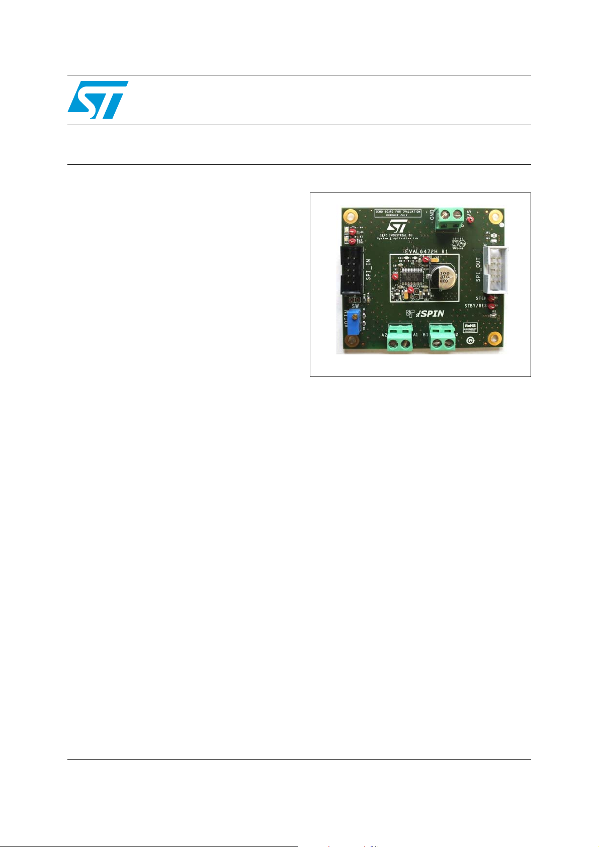
EVAL6472H
Features
■ Voltage range from 8 V to 45 V
■ Phase current up to 3 A
SPI with daisy chain feature
■
■ SW input
■ FLAG and BUSY LED indicators
■ Adjustable supply voltage compensation
■ Suitable for use in combination with STEVAL-
PCC009V2
Description
r.m.s.
EVAL6472H
Data brief
The EVAL6472H demonstration board is a fully
integrated microstepping motor driver. In
combination with the STEVAL-PCC009V2
communication board and the dSPIN evaluation
software, the board allows the user to investigate
all the features of the L6472 device. In particular,
the board can be used to regulate the L6472
parameters in order to fit application
requirements.
The EVAL6472H supports the daisy chain
configuration making it suitable for the evaluation
of the L6472 in the multi-motor applications.
March 2012 Doc ID 022980 Rev 1 1/11
For further information contact your local STMicroelectronics sales office.
www.st.com
11
Page 2
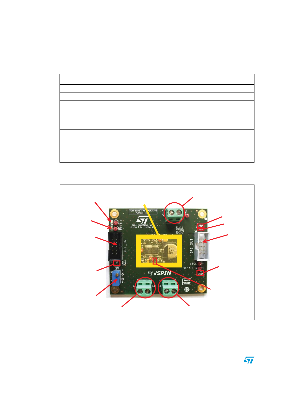
Board description EVAL6472H
Phase A connector
Power supply connector
(8 V - 45 V )
Master SPI
connector
BUSY LED
(Amber)
FLAG LED
(Red)
Motor supply voltage
compensation
partitioning regulation
(ADCIN input)
External switch connector
(SW input)
JP1: VDD supply from
master SPI connector
JP2: VDD to VREG
connection
OSCIN/OSCOUT
connector
JP3: Daisy chain
termination
Phase B connector
Slave SPI
connector
Application reference
area
AM10289V1
1 Board description
Table 1. EVAL6472H specifications
Parameter Value
Supply voltage (VS) 8 to 45 V
Maximum output current (each phase) 3 A
Logic supply voltage (VREG)
Externally supplied: 3.3 V
Internally supplied: 3 V typical
r.m.s.
Logic interface voltage (VDD)
Externally supplied: 3.3 V or 5 V
Internally supplied: VREG
Low level logic input voltage 0 V
High level logic input voltage VDD
Operating temperature -25 to +125 °C
L6472H thermal resistance junction-to-ambient 21 °C/W typical
1. All logic inputs are 5 V tolerant.
Figure 1. Jumpers and connectors location
(1)
2/11 Doc ID 022980 Rev 1
Page 3

EVAL6472H Board description
Table 2. Jumpers and connectors description
Name Type Function
M1 Power supply Motor supply voltage
M2 Power output Bridge A outputs
M3 Power output Bridge B outputs
CN1 SPI connector Master SPI
CN2 SPI connector Slave SPI
CN3 NM connector OSCIN and OSCOUT pins
CN4 NM connector External switch input
TP1 (VS) Test point Motor supply voltage test point
TP2 (VDD) Test point Logic interface supply voltage test point
TP3 (VREG) Test point
TP5 (GND) Test point Ground test point
TP6 (GND) Test point Ground test point
Logic supply voltage/L6470 internal regulator test
point
TP8 (STCK) Test point Step clock input test point
TP9 (STBY/RES) Test point Standby/reset input test point
TP10 (FLAG) Test point FLAG output test point
TP11
(BUSY/SYNC)
Test point BUSY/SYNC output test point
Table 3. Master SPI connector pinout (J10)
Pin
number
1 Open drain output L6472 BUSY output
2 Open drain output L6472 FLAG output
3 Ground Ground
4 Supply EXT_VDD (can be used as external logic power supply)
5 Digital output
6 Digital input SPI serial clock signal (connected to L6472 CK input)
7 Digital input
8 Digital input SPI slave select signal (connected to L6472 CS input)
Type Description
SPI master IN slave OUT signal (connected to L6472 SDO
output through daisy chain termination jumper JP2)
SPI master OUT slave IN signal (connected to L6472 SDI
input)
9 Digital input L6472 step-clock input
10 Digital input L6472 standby/reset input
Doc ID 022980 Rev 1 3/11
Page 4
Board description EVAL6472H
Table 4. Slave SPI connector pinout (J11)
Pin
number
1 Open drain output L6472 BUSY output
2 Open drain output L6472 FLAG output
3 Ground Ground
4 Supply EXT_VDD (can be used as external logic power supply)
5 Digital output SPI master IN slave OUT signal (connected to pin 5 of J10)
6 Digital input SPI serial clock signal (connected to L6472 CK input)
7 Digital input
8 Digital input SPI slave select signal (connected to L6472 CS input)
9 Digital input L6472 step-clock input
10 Digital input L6472 standby/reset input
Type Description
SPI master OUT slave IN signal (connected to L6472 SDO
output)
4/11 Doc ID 022980 Rev 1
Page 5

EVAL6472H Board description
1A
2A
SW
1B
2B
OSCIN OSCOUT
Application reference
VS
GND
OPTION
SE
R
/YBTSKCTS
TUO_IPSNI_IP
S
YSUBGALF
GND
VDD
VREG
VS
SW
MISO
SDI
CK
nCS
FLAG
BUSY
STCK
STBY_RESET
MISO
SDO
CK
nCS
FLAGBUSY
SDO
MISO
BUSY
SDI
CK
nCS
SW
ADCIN
SDO
BUSYFLAG
FLAG
STBY_RESETSTCK
STCK
STBY_RESET
VS
VS
EXT_VDD EXT_VDD
EXT_VDD
VDD
VREG
VREG
VDD
VREG
VDD
VS
VDD
VDD VDD
VS
VS
J6
MORSV-508-2P
1
2
J4
NM
1
2
C10
100pF/6V3
J2
1
234
567
8910
J1
MORSV-508-2P
1
2
TP1
1
DL2
YELLOW
2 1
C6
10nF/50V
D1
BAV99
12
3
JP3
DL1
RED
2
1
C1
220nF/16V
C15
100nF/50V
R9
470
C12
100pF/6V3
TP7
1
TP8
1
C14
10nF/6V3
U1
L6472
VDD
17
VREG
6
OSCIN7OSCOUT
8
CP
10
VBOOT
11
ADCIN
5
VSA
2
VSA
26
VSB
12
VSB
16
PGND
13
PGND
27
OUT1A
1
OUT2A
28
OUT1B
14
OUT2B
15
AGND
9
SW
4
DGND
21
BUSY_SYNC
22
FLAG24SDO18SDI
20
CK
19
CS
23
STBY_RES
3
STCK
25
EPAD
29
TP4
1
C4
100nF/6V3
+
C5
47uF/6V3
C8
100nF/50V
R8
100
R2
200K
1 3
2
+
C3
10uF/6V3
R1
31k6
R5
39k
R7
470
+
C9A
100uF/63V
J5
MORSV-508-2P
1
2
TP3
1
C13
3.3nF/6V3
D2
BZX585-B3V6
TP5
1
C7
100nF/50V
R6
39k
TP6
1
J3
12345
6
7
8
9
10
C16
100nF/50V
C11
100pF/6V3
JP2
TP2
1
C2
100nF/6V3
R4
39k
J7
NM
1
2
R3
8k2
+
C9
100uF/63V
JP1
AM10295V1
Figure 2. EVAL6472H schematic
Doc ID 022980 Rev 1 5/11
Page 6

Board description EVAL6472H
Table 5. Bill of material
Index Quantity Reference Value Package
1 1 C1 220 nF/16 V CAPC-0603
2 2 C2,C4 100 nF/6V3 CAPC-0603
3 1 C3 10 µF/6V3 CAPC-3216
4 1 C5 47 µF/6V3 CAPC-3216
5 1 C6 10 nF/50 V CAPC-0603
6 4 C7, C8, C15, C16 100 nF/50 V CAPC-0603
7 1 C9A 100 µF/6V3 (option) CAPE-R10HXX-P5
8 1 C9 100 µF/6V3 CAPES-R10HXX
9 3 C10, C11, C12 100 pF/6V3 CAPC-0603
10 1 C13 3.3 nF/6V3 CAPC-0603
11 1 C14 10 nF/6V3 CAPC-0603
12 1 DL1 LED diode (red) LEDC-0805
13 1 DL2 LED diode (amber) LEDC-0805
14 1 D1 BAV99 SOT23
15 1 D2 BZX585-B3V6 SOD323
16 1 JP1 Jumper - open JP2SO
17 2 JP2, JP3 Jumper - closed JP2SO
18 3 J1, J5, J6 Screw connector 2 poles MORSV-508-2P
19 2 J2,J3
20 2 J4, J7 NM STRIP254P-M-2
21 1 R1 31.6 kΩ RESC-0603
22 1 R2 200 kΩ TRIMM-100X50X110-64W
23 1 R3 8.2 kΩ RESC-0603
24 3 R4, R5, R6 39 kΩ RESC-0603
25 2 R7, R9 470 Ω RESC-0603
26 1 R8 100 Ω RESC-0603
TP1, TP2, TP3,
27 7
28 1 TP6 TPTH-ring-1 mm black TH
29 1 U1 L6472 HTSSOP28
TP4, TP5, TP7,
TP8
Pol. IDC male header vertical
10 poles
TPTH-ring-1 mm red TH
CON-FLAT-5X2-180M
6/11 Doc ID 022980 Rev 1
Page 7

EVAL6472H Board description
AM10290V2
AM10290V1
Figure 3. EVAL6472H - silkscreen
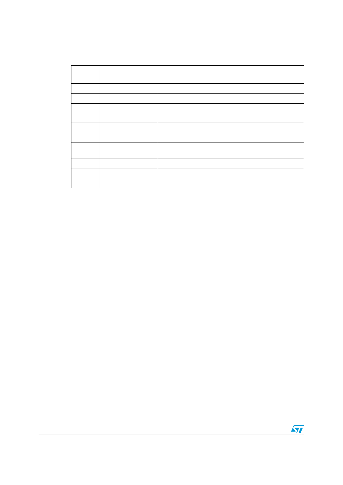
Figure 4. EVAL6472H - layout (top layer)
Doc ID 022980 Rev 1 7/11
Page 8
Board description EVAL6472H
AM10291V1
AM10292V1
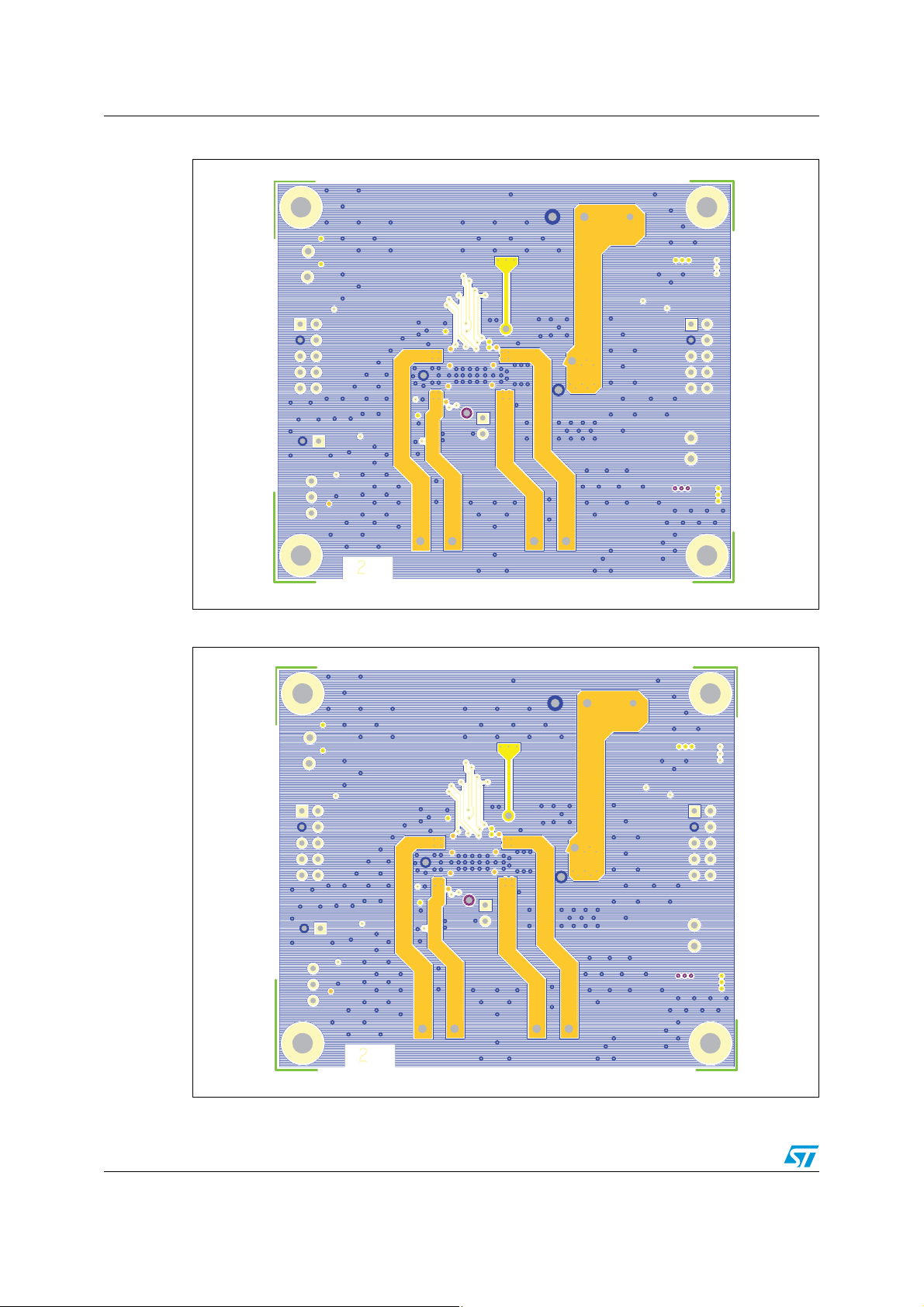
Figure 5. EVAL6472H - layout (inner layer2)
Figure 6. EVAL6472H - layout (inner layer3)
8/11 Doc ID 022980 Rev 1
Page 9

EVAL6472H Board description
AM10293V1
1
10
100
1000
Time (sec)
0
5
10
15
20
25
Zth (°C/W)
AM10294V1
Figure 7. EVAL6472H - layout (bottom layer3)
1.1 Thermal data
Figure 8. Thermal impedance graph
Doc ID 022980 Rev 1 9/11
Page 10

Revision history EVAL6472H
2 Revision history
Table 6. Document revision history
Date Revision Changes
21-Mar-2012 1 Initial release.
10/11 Doc ID 022980 Rev 1
Page 11

EVAL6472H
Please Read Carefully:
Information in this document is provided solely in connection with ST products. STMicroelectronics NV and its subsidiaries (“ST”) reserve the
right to make changes, corrections, modifications or improvements, to this document, and the products and services described herein at any
time, without notice.
All ST products are sold pursuant to ST’s terms and conditions of sale.
Purchasers are solely responsible for the choice, selection and use of the ST products and services described herein, and ST assumes no
liability whatsoever relating to the choice, selection or use of the ST products and services described herein.
No license, express or implied, by estoppel or otherwise, to any intellectual property rights is granted under this document. If any part of this
document refers to any third party products or services it shall not be deemed a license grant by ST for the use of such third party products
or services, or any intellectual property contained therein or considered as a warranty covering the use in any manner whatsoever of such
third party products or services or any intellectual property contained therein.
UNLESS OTHERWISE SET FORTH IN ST’S TERMS AND CONDITIONS OF SALE ST DISCLAIMS ANY EXPRESS OR IMPLIED
WARRANTY WITH RESPECT TO THE USE AND/OR SALE OF ST PRODUCTS INCLUDING WITHOUT LIMITATION IMPLIED
WARRANTIES OF MERCHANTABILITY, FITNESS FOR A PARTICULAR PURPOSE (AND THEIR EQUIVALENTS UNDER THE LAWS
OF ANY JURISDICTION), OR INFRINGEMENT OF ANY PATENT, COPYRIGHT OR OTHER INTELLECTUAL PROPERTY RIGHT.
UNLESS EXPRESSLY APPROVED IN WRITING BY TWO AUTHORIZED ST REPRESENTATIVES, ST PRODUCTS ARE NOT
RECOMMENDED, AUTHORIZED OR WARRANTED FOR USE IN MILITARY, AIR CRAFT, SPACE, LIFE SAVING, OR LIFE SUSTAINING
APPLICATIONS, NOR IN PRODUCTS OR SYSTEMS WHERE FAILURE OR MALFUNCTION MAY RESULT IN PERSONAL INJURY,
DEATH, OR SEVERE PROPERTY OR ENVIRONMENTAL DAMAGE. ST PRODUCTS WHICH ARE NOT SPECIFIED AS "AUTOMOTIVE
GRADE" MAY ONLY BE USED IN AUTOMOTIVE APPLICATIONS AT USER’S OWN RISK.
Resale of ST products with provisions different from the statements and/or technical features set forth in this document shall immediately void
any warranty granted by ST for the ST product or service described herein and shall not create or extend in any manner whatsoever, any
liability of ST.
ST and the ST logo are trademarks or registered trademarks of ST in various countries.
Information in this document supersedes and replaces all information previously supplied.
The ST logo is a registered trademark of STMicroelectronics. All other names are the property of their respective owners.
© 2012 STMicroelectronics - All rights reserved
STMicroelectronics group of companies
Australia - Belgium - Brazil - Canada - China - Czech Republic - Finland - France - Germany - Hong Kong - India - Israel - Italy - Japan -
Malaysia - Malta - Morocco - Philippines - Singapore - Spain - Sweden - Switzerland - United Kingdom - United States of America
www.st.com
Doc ID 022980 Rev 1 11/11
 Loading...