

Page 1
Dual full bridge with programmable overcurrent
Features
■ Voltage range from 8 V to 52 V
■ Phase current up to 2.5 Ar.m.s.
■ Adjustable overcurrent threshold
■ Logic inputs 5 V / 3.3 V compliant
■ Small application footprint with high thermal
performance
■ Suitable for use in combination with
PractiSPIN™ 2 software
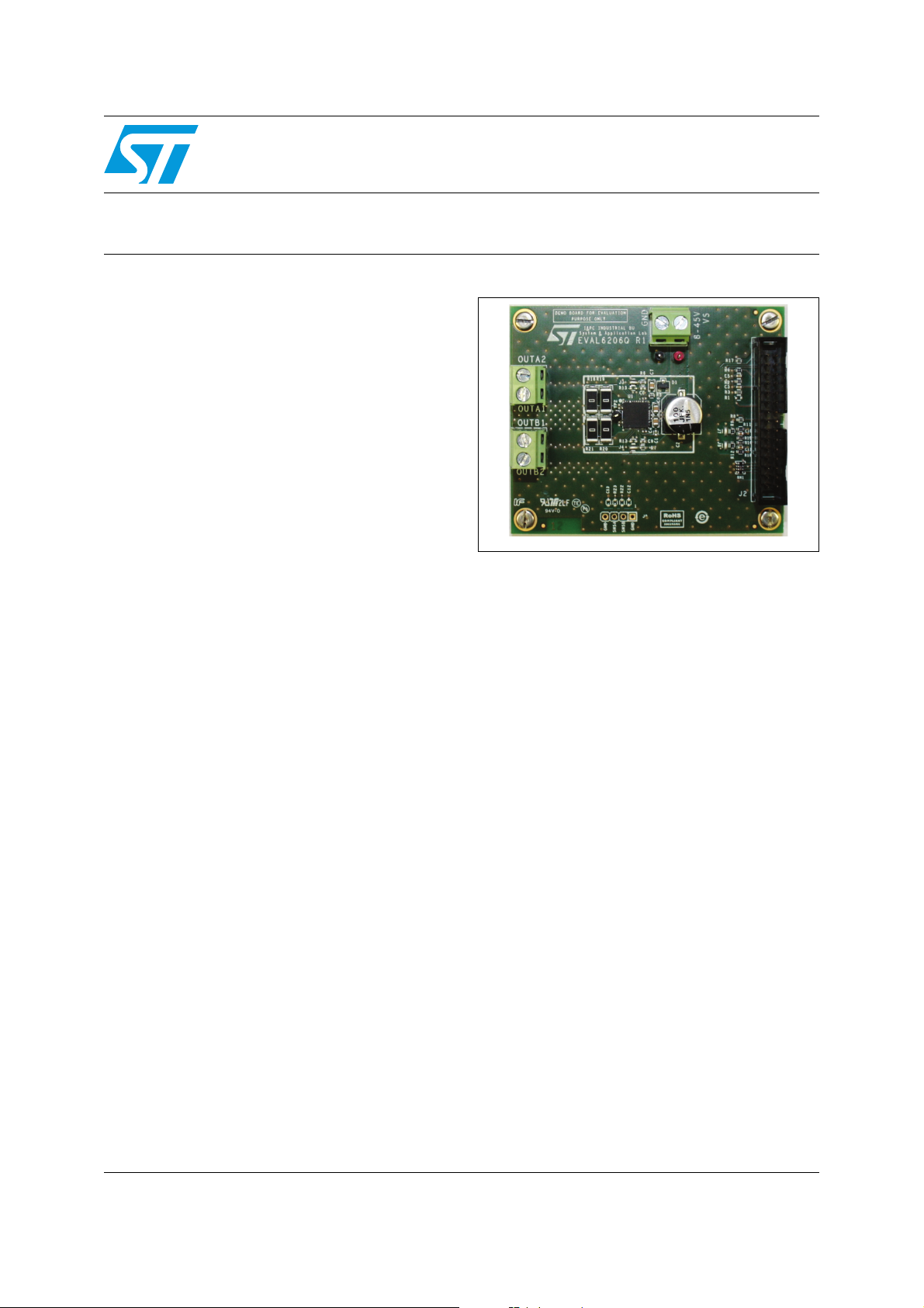
EVAL6206Q
Data brief
Description
The EVAL6206Q demonstration board allows the
user to test the L6206Q functions. The dual full
bridges integrated into the L6206Q can be used
to drive a single 2-phase stepper motor or up to
four DC motors (unidirectional). The bridges can
also operate in parallel mode. The board can be
driven using the STEVAL-PCC009V2
communication board and the PractiSPIN 2
evaluation software.
AM11895v1
April 2012 Doc ID 023042 Rev 1 1/10
For further information contact your local STMicroelectronics sales office.
www.st.com
10
Page 2
Board description EVAL6206Q
1 Board description
Table 1. EVAL6206Q electrical specifications
Parameter Value
Supply voltage (VS) 8 to 52 V
Maximum output current (each phase) 2.5 Ar.m.s.
Low level logic input voltage 0 V
High level logic input voltage 5 V / 3.3 V
Switching frequency up to 100 kHz
Operating temperature - 25 to +125 °C
L6206Q thermal resistance junction-to-ambient TBD
1. Logic inputs are 3.3 V and 5 V compliant.
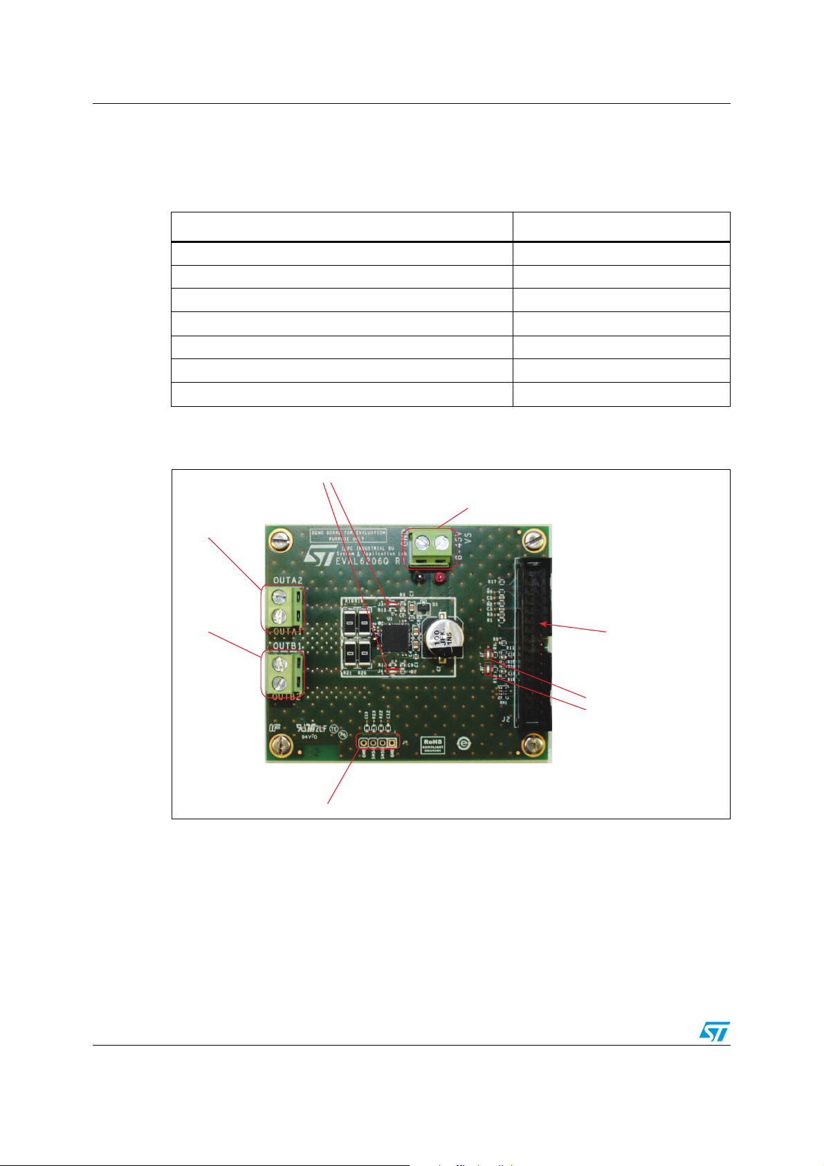
Figure 1. Trimmer and connector locations
J3 and J4: OCDX to ENX pin connection
P
ower supply connector
(8 V - 52 V)
(1)
Phase A connector
Phase B connector
Current sensing connector
C
ontrol board
connector
J7 and J8
OCD theshold regulation
CLOSED -
through control board.
OPEN - OCD threshold regulation
through R13 and R15
resistors (not mounted)
AM11896v1
2/10 Doc ID 023042 Rev 1
Page 3

EVAL6206Q Board description
Table 2. Control board connector pinout (J2)
Pin Type Function
2 Ground Ground
3 Logic input Input IN1A of L6206Q
4 Logic input Input IN2A of L6206Q
5 Logic input Input IN1B of L6206Q
6 Logic input Input IN2B of L6206Q
11 Analog input Overcurrent threshold regulation for A bridge
12 Analog input Overcurrent threshold regulation for B bridge
13 Ground Ground
14 Supply voltage 3.3 V supply voltage
16 Logic input Input ENA of L6206Q
23 Ground Ground
24 Analog output Board identification system ID0
25 Analog output Board identification system ID1
27 Logic output Fault output for A bridge (OCDA output of L6206Q)
28 Ground Ground
29 Logic output Fault output for B bridge (OCDB output of L6206Q)
30 Logic input Input ENB of L6206Q
Others Unconnected
Table 3. Current sensing connector (J9)
Pin Type Function
1 Ground Ground
2 Analog output SENSEA pin of L6206Q
3 Analog output SENSEB pin of L6206Q
4 Ground Ground
1. R22/23 resistor and C12/13 capacitor must be added when output is used. The value of the RC network
should be chosen according to the target low-pass frequency of the filter.
(1)
(1)
Doc ID 023042 Rev 1 3/10
Page 4

Board description EVAL6206Q
Figure 2. EVAL6206Q - schematic
OUT1A
PTH OPTION
220n/16V
C1
OUT2A
J5
1
2
C2A
OPTION
+
VS
21
VBOOT
10n/100V
C7
3
D1
BAV99
1 2
C6
100n/100V
R5 100
40
VCP
35
VSA
34
VSA
27
VSB
26
VSB
U1
39
3
OUT1A#22OUT1A#3
OUT2A#3838OUT2A#39
L6206Q
ENA41IN1A43IN2A
OCDA48OCDB
20
44
13
OUT2B
OUT1B
J6
1
2
11
23
OUT1B#1010OUT1B#11
OUT2B#2222OUT2B#23
IN1B17IN2B
ENB
PROGCLB
PROGCLA42NC#11NC#44NC#55NC#77NC#88NC#99NC#1212NC#1414NC#24
18
19
47
NC#2525NC#2828NC#2929NC#3030NC#3232NC#3333NC#3636NC#3737NC#47
24
16
SNSB#16
15
SNSB#15
46
SNSA#46
45
SNSA#45
31
GND
6
GND
49
EPAD
SENSEBSENSEA
R21
R20
R19
R18
0/1W
0/1W
0/1W
0/1W
VS
Application reference
R2
10k/1%
3V3 3V3
NM
R1
1
VS GND
1
VS
1
2
J1
VS
GND
+
C2
ID1
ID0
52V - 8V
C4
100n/100V
100u/63V
C5
100n/4V
R4
14k/1%
C3
100n/4V
0
R3
OCDA
J3
1 2
R6 100k
1 8
4 5
3 6
2 7
RN1A 56K
RN1D 56K
RN1C 56K
RN1B 56K
IN1A
IN2A
IN1B
IN2B
1234567891011121314151617181920212223242526272829
J2
ENA
IN1A
IN2A
C8
3V3
OCDB
J4
1 2
5.6n/6V3
R7 100k
ENB
IN1B
IN2B
C9
5.6n/6V3
J7
R9 1k5
R10 12k
ENA
1 2
C10
68n/6V3
5k6
R11
R8
10k
ID0
ID1
R13
R15
J8
1 2
R12 1k5
R14 12k
OCDB
NM
NM
C11
R16
ENB
OCDA
30
68n/6V3
5k6
R17
1
GND
SENSEA
SENSEB
NM
NM
R23
R22
10k
123
J9
SNSA
SNSB
C13
NM
C12
NM
4
AM11897v1
4/10 Doc ID 023042 Rev 1
Page 5

EVAL6206Q Board description
Table 4. EVAL6206Q - Bill of material
Index Quantity Reference Value Package
1 1 C1 220 nF / 16 V CAPC-0603
2 1 C2 100 µF / 63 V CAPES-R10HXX
3 1 C2A 100 µF / 63 V (OPTION) CAPE-R8H12-P35
4 2 C3,C5 100 nF / 4 V CAPC-0603
5 2 C4,C6 100 nF / 100 V CAPC-0805
6 1 C7 10 nF / 100 V CAPC-0805
7 2 C8,C9 5.6 nF / 6V3 CAPC-0603
8 2 C10,C11 68 nF / 6V3 CAPC-0603
9 2 C12,C13 NM CAPC-0603
10 1 D1 BAV99 SOT-23
11 3 J1,J5,J6 Screw connector 2 poles MORSV-508-2P
12 1 J2
13 4 J3,J4,J7,J8 Jumper - CLOSE JP2SO
14 1 J9 NM STRIP254P-M-4
15 1 RN1 56 kΩ RESN-CAY16
16 5 R1,R13,R15,R22,R23 NM RESC-0603
17 1 R2 10 kΩ / 1% RESC-0603
18 1 R3 0 Ω RESC-0603
19 1 R4 14 kΩ / 1% RESC-0603
20 1 R5 100 Ω RESC-0603
21 2 R6,R7 100 kΩ RESC-0603
22 2 R8,R17 10 kΩ RESC-0603
23 2 R9,R12 1.5 kΩ RESC-0603
24 2 R10,R14 12 kΩ RESC-0603
25 2 R11,R16 5.6 kΩ RESC-0603
26 4 R18,R19,R20,R21 0 Ω / 1 Ω RESC-2512
27 1 TP1 TPTH-RING-1MM RED TH
28 2 TP2,TP3
29 1 U1 L6206Q QFN (7x7_48)
Pol. IDC male header
vertical 30 poles
TPTH-RING-1MM
BLACK
CON-FLAT-15X2-180M
TH
Doc ID 023042 Rev 1 5/10
Page 6

Board description EVAL6206Q
Figure 3. EVAL6206Q - layout (silk screen)
AM11898v1
Figure 4. EVAL6206Q - layout (top layer)
AM11899v1
6/10 Doc ID 023042 Rev 1
Page 7

EVAL6206Q Board description
Figure 5. EVAL6206Q - layout (inner layer 2)
AM11900v1
Figure 6. EVAL6206Q - layout (inner layer 3)
AM11901v1
Doc ID 023042 Rev 1 7/10
Page 8

Board description EVAL6206Q
Figure 7. EVAL6206Q - layout (bottom layer)
AM11902v1
Figure 8. Overcurrent threshold regulation
AM11903v1
8/10 Doc ID 023042 Rev 1
Page 9

EVAL6206Q Revision history
2 Revision history
Table 5. Document revision history
Date Revision Changes
03-Apr-2012 1 Initial release.
Doc ID 023042 Rev 1 9/10
Page 10

EVAL6206Q
Please Read Carefully:
Information in this document is provided solely in connection with ST products. STMicroelectronics NV and its subsidiaries (“ST”) reserve the
right to make changes, corrections, modifications or improvements, to this document, and the products and services described herein at any
time, without notice.
All ST products are sold pursuant to ST’s terms and conditions of sale.
Purchasers are solely responsible for the choice, selection and use of the ST products and services described herein, and ST assumes no
liability whatsoever relating to the choice, selection or use of the ST products and services described herein.
No license, express or implied, by estoppel or otherwise, to any intellectual property rights is granted under this document. If any part of this
document refers to any third party products or services it shall not be deemed a license grant by ST for the use of such third party products
or services, or any intellectual property contained therein or considered as a warranty covering the use in any manner whatsoever of such
third party products or services or any intellectual property contained therein.
UNLESS OTHERWISE SET FORTH IN ST’S TERMS AND CONDITIONS OF SALE ST DISCLAIMS ANY EXPRESS OR IMPLIED
WARRANTY WITH RESPECT TO THE USE AND/OR SALE OF ST PRODUCTS INCLUDING WITHOUT LIMITATION IMPLIED
WARRANTIES OF MERCHANTABILITY, FITNESS FOR A PARTICULAR PURPOSE (AND THEIR EQUIVALENTS UNDER THE LAWS
OF ANY JURISDICTION), OR INFRINGEMENT OF ANY PATENT, COPYRIGHT OR OTHER INTELLECTUAL PROPERTY RIGHT.
UNLESS EXPRESSLY APPROVED IN WRITING BY TWO AUTHORIZED ST REPRESENTATIVES, ST PRODUCTS ARE NOT
RECOMMENDED, AUTHORIZED OR WARRANTED FOR USE IN MILITARY, AIR CRAFT, SPACE, LIFE SAVING, OR LIFE SUSTAINING
APPLICATIONS, NOR IN PRODUCTS OR SYSTEMS WHERE FAILURE OR MALFUNCTION MAY RESULT IN PERSONAL INJURY,
DEATH, OR SEVERE PROPERTY OR ENVIRONMENTAL DAMAGE. ST PRODUCTS WHICH ARE NOT SPECIFIED AS "AUTOMOTIVE
GRADE" MAY ONLY BE USED IN AUTOMOTIVE APPLICATIONS AT USER’S OWN RISK.
Resale of ST products with provisions different from the statements and/or technical features set forth in this document shall immediately void
any warranty granted by ST for the ST product or service described herein and shall not create or extend in any manner whatsoever, any
liability of ST.
ST and the ST logo are trademarks or registered trademarks of ST in various countries.
Information in this document supersedes and replaces all information previously supplied.
The ST logo is a registered trademark of STMicroelectronics. All other names are the property of their respective owners.
© 2012 STMicroelectronics - All rights reserved
STMicroelectronics group of companies
Australia - Belgium - Brazil - Canada - China - Czech Republic - Finland - France - Germany - Hong Kong - India - Israel - Italy - Japan -
Malaysia - Malta - Morocco - Philippines - Singapore - Spain - Sweden - Switzerland - United Kingdom - United States of America
www.st.com
10/10 Doc ID 023042 Rev 1
 Loading...