

www.DataSheet4U.com
ESDALC6V1xxM6
4 and 5 line low capacitance TRANSIL™ array for ESD protection
Main applications
Where transient overvoltage protection in ESD
sensitive equipment is required, such as:
■ Computers
■ Printers
■ Communication systems
■ Cellular phone handsets and accessories
■ Video equipment
Features
■ 4 unidirectional TRANSIL diodes
(ESDALC6V1M6)
■ 5 unidirectional TRANSIL diodes
(ESDALC6V1-5M6)
■ Breakdown Voltage V
■ Low diode capacitance (12 pF typ at 0 V)
■ Low leakage current < 70 nA
■ Very small PCB area: 1.45 mm
■
500 microns pitch
■ Leadfree package
= 6.1 V min
BR
²
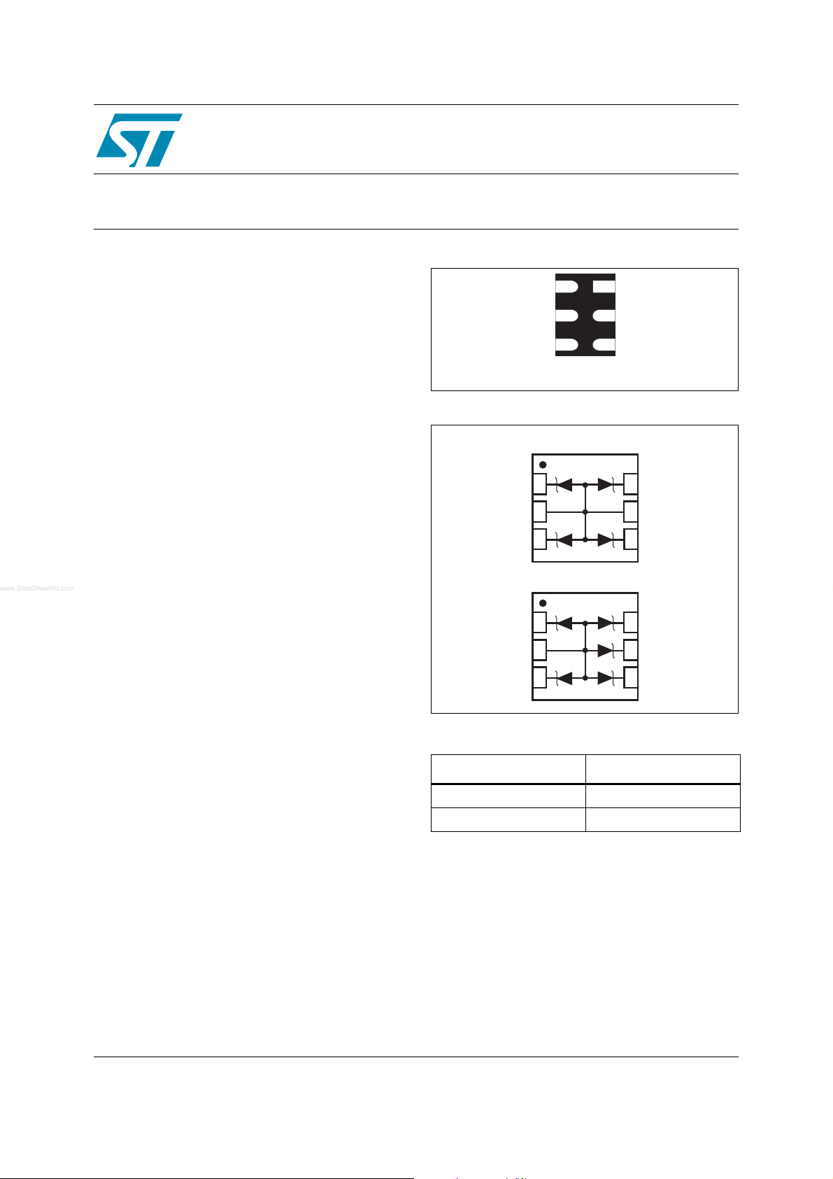
Functional diagram
Micro QFN Package
ESDALC6V1M6
1
I/O1
2
GND
I/O2
3
ESDALC6V1-5M6
1
I/O1
2
GND
I/O2
3
6
5
4
6
5
4
I/O5
GND
I/O3
I/O5
I/O4
I/O3
Description
The ESDALC6V1xxM6 is monolithic arrays
designed to protect up to 4 or 5 lines against ESD
transients.
The device is ideal for applications where both
reduced print circuit board space and power
absorption capability are required.
Benefits
■ High ESD protection level
■ High integration
■ Suitable for high density boards
January 2006 1/8
Order Code
Part number Marking
ESDALC6V1M6 G
ESDALC6V1-5M6 H
Complies with the following standards:
IEC61000-4-2
15 kV (air discharge)
8 kV (contact discharge)
MIL STD 883E- Method 3015-7: class3
25 kV (human body model)
TM: TRANSIL is a trademark of STMicroelectronics
Rev 3
www.st.com
8
1 Characteristics ESDALC6V1xxM6
1 Characteristics
1.1 Absolute maximum ratings (T
Symbol Parameter Value Unit
V
PP
P
PP
I
pp
T
T
stg
T
L
T
OP
1. For a surge greater than the maximum values, the diode will fail in short-circuit.
1.2 Electrical characteristics (T
Symbol Parameter
V
RM
V
BR
V
CL
I
RM
I
PP
αT Voltage temperature coefficient
V
F
ESD discharge – IEC61000-4-2 air discharge
IEC61000-4-2 contact discharge
Peak pulse power dissipation (8/20 µs)
Repetitive peak pulse current typical value (8/20 µs) 3 A
Junction temperature 125 °C
j
Storage temperature range -55 + 150 °C
Maximum lead temperature for soldering during 10 s 260 °C
Operating temperature range -40 + 125 °C
amb
Stand-off voltage
Breakdown voltage
Clamping voltage
Leakage current @ V
Peak pulse current
Forward voltage drop
RM
= 25 °C)
amb
(1)
= 25 °C)
Tj initial = T
VV V
BR
RM
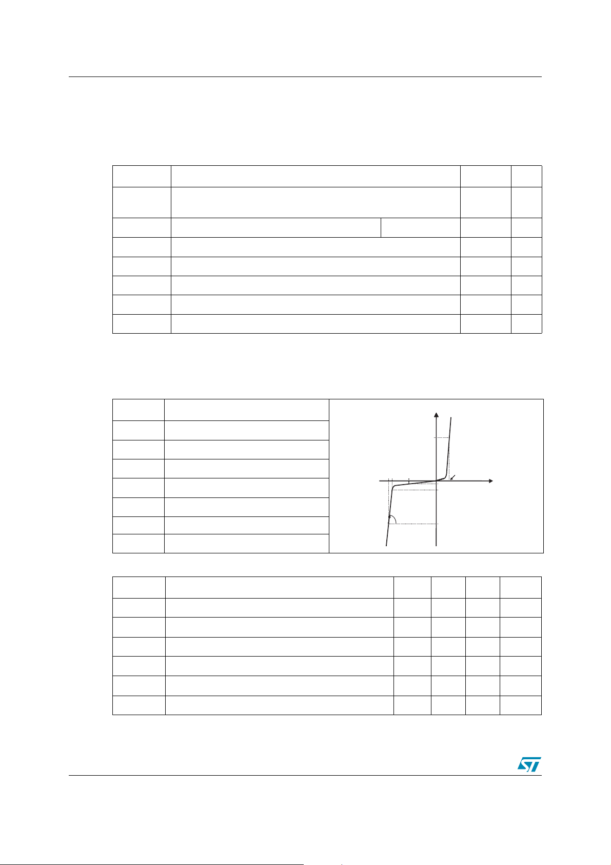
Slope= 1/R
± 15
± 8
V
F
30 W
V
V
VVCLV
V
amb
I
I
F
I
RM
I
R
d
I
PP
kV
Parameter Test Condition Min Typ Max Unit
V
BR
I
RM
V
F
R
d
(1)
αT
C
1. ∆VBR = αT * (T
V
=0 V DC, F = 1 MHz, V
R
- 25 °C) * VBR (25 °C)
amb
IR = 1 mA
V
= 3 V
RM
IF = 10 mA
IR = 1 mA,
osc
2/8
= 30 mV
RMS
6.1 7.2 V
70 nA
1V
23 Ω
5
10
12 15 pF
-4
/°C
ESDALC6V1xxM6 1 Characteristics
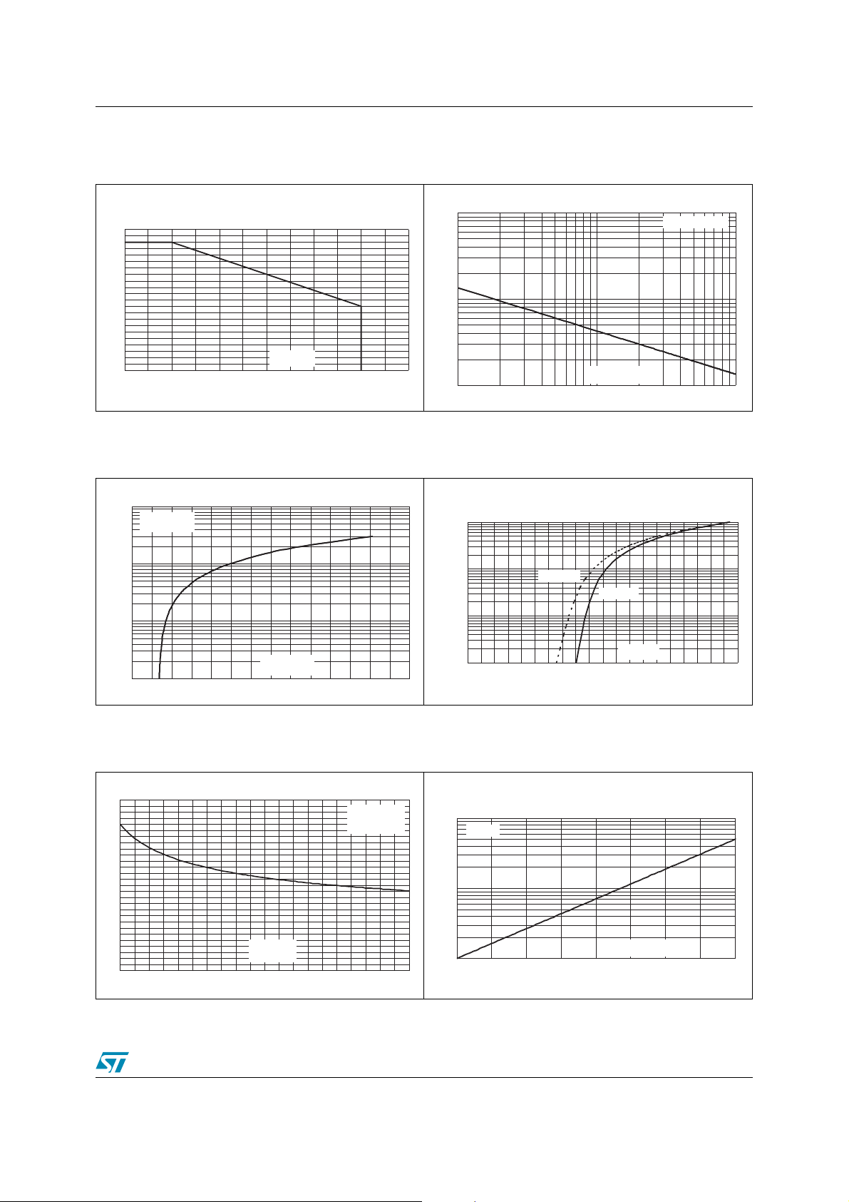
Figure 1. Relative variation of peak pulse
power versus initial junction
temperature
PPP[Tjinitial] /PPP[Tjinitial=25 ]
1.1
1.0
0.9
0.8
0.7
0.6
0.5
0.4
0.3
0.2
0.1
0.0
0 25 50 75 100 125 150
°C
Tj(°C)
Figure 3. Clamping voltage versus peak pulse
current (typical values, rectangular
waveform)
IPP(A)
IPP(A)
100.0
100.0
8/20µs
8/20µs
initial =25°C
initial =25°C
T
T
j
j
Figure 2. Peak pulse power versus
exponential pulse duration
PPP(W)
PPP(W)
1000
1000
100
100
10
10
1 10 100
1 10 100
tP(µs)tP(µs)
Tjinitial = 25°C
Tjinitial = 25°C
Figure 4. Forward voltage drop versus peak
forward current (typical values)
IFM(A)
1.E+00
10.0
10.0
1.0
1.0
0.1
0.1
0 10203040506070
0 10203040506070
VCL(V)VCL(V)
Figure 5. Junction capacitance vesus reverse
voltage applied (typical values)
C(pF)C(pF)
14
13
12
11
10
9
8
7
6
5
4
3
2
1
0
0.0 0.5 1.0 1.5 2.0 2.5 3.0 3.5 4.0 4.5 5.0
VR(V)VR(V)
V
F=1MHz
OSC
Tj=25°C
=30mV
RMS
1.E-01
1.E-02
1.E-03
0.0 0.2 0.4 0.6 0.8 1.0 1.2 1.4 1.6 1.8 2.0
Tj=125°C
Tj=25°C
VFM(V)
Figure 6. Relative variation of leakage current
versus junction temperature (typical
values)
IR[Tj]/IR[Tj=25 ]
100
10
1
25 50 75 100 125
°C
VR=3V
Tj(°C)
3/8
 Loading...