ST ESDALC6V1P5 Service Manual

www.DataSheet4U.com
®
QUAD LOW CAPACITANCE TRANSIL™
Application Specific Discretes
A.S.D.
MAIN APPLICATIONS
Where transient overvoltage protection in ESD
sensitive equipment is required, such as :
Computers
■
Printers
■
Communication systems and cellular phones
■
Video equipment
■
This device is particularly adapted to the protection
of symmetrical signals.
FEATURES
4 UNIDIRECTIONAL TRANSIL™ FUNCTIONS.
■
BREAKDOWN VOLTAGE VBR= 6.1V MIN.
■
LOW DIODE CAPACITANCE (12pF @ 0V)
■
LOW LEAKAGE CURRENT < 100 nA
■
VERY SMALL PCB AREA < 2.6 mm
■
2
ESDALC6V1P5
ARRAY FOR ESD PROTECTION
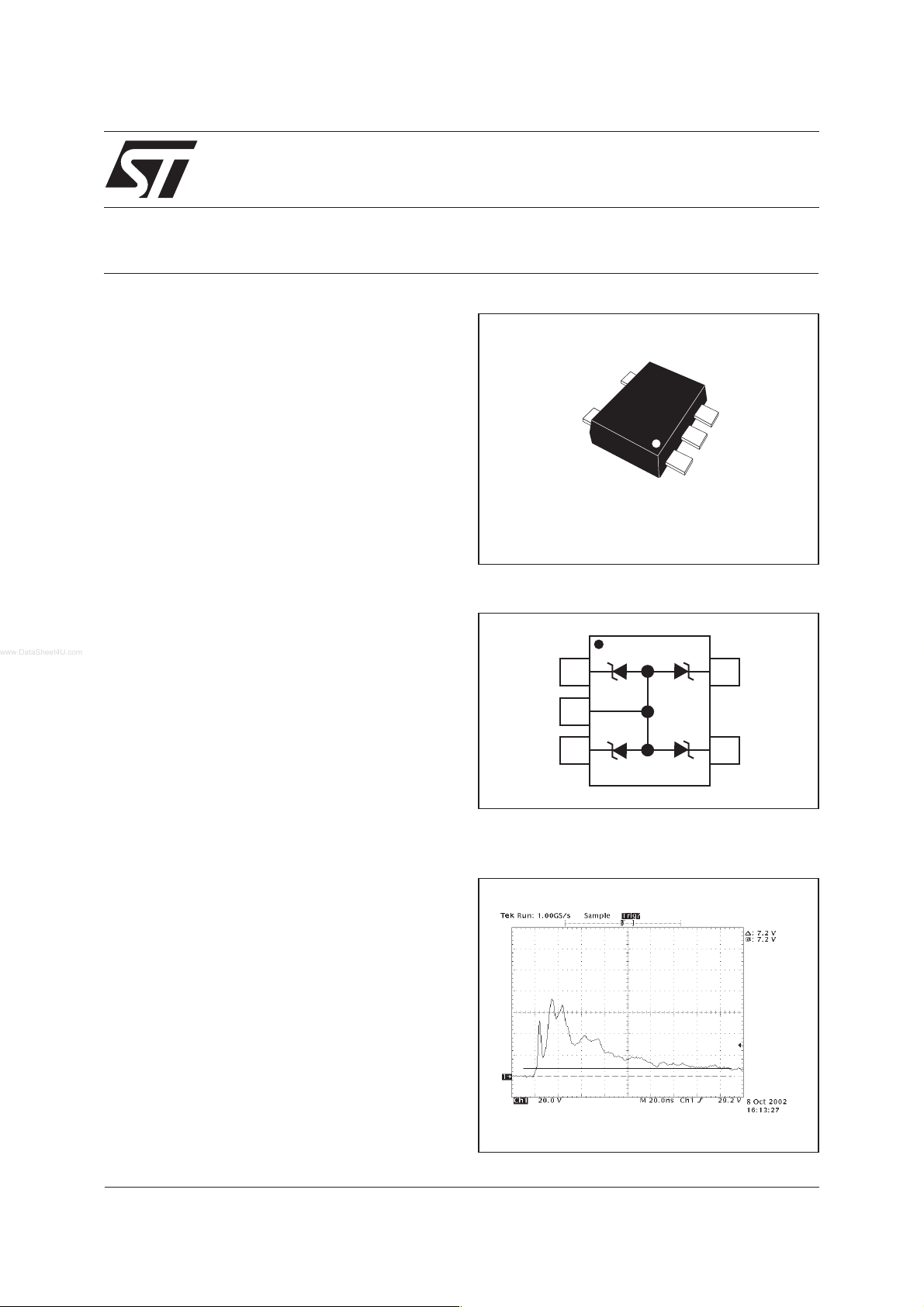
SOT665
(Jedec SC89-5L)
FUNCTIONAL DIAGRAM
DESCRIPTION
The ESDALC6V1P5 is a monolithic array designed
to protect up to 4 lines against ESD transients.
This device is ideal for applications where both
reduced line capacitance and board space saving
are required.
BENEFITS
■
High ESD protection level.
■
High integration.
■
Suitable for high density boards.
COMPLIES WITH THE FOLLOWING STANDARDS :
■
IEC61000-4-2 level 4: 15 kV (air discharge)
8 kV (contact discharge)
■
MIL STD 883E-Method 3015-7: class 3
25kV HBM (Human Body Model)
1
5
2
3
ESD response to IEC61000-4-2 level 4 (15kV
contact)
4
February 2004 - Ed: 1
1/5

ESDALC6V1P5
ABSOLUTE RATINGS (T
amb
= 25°C)
Symbol Parameter Test conditions Value Unit
V
PP
P
PP
T
j
T
stg
T
L
T
op
Note 1: for a surge greater than the maximum values, the diode will fail in short-circuit.
ESD discharge - IEC61000-4-2 air discharge
IEC61000-4-2 contact discharge
Peak pulse power (8/20 µs) (see note 1) Tjinitial = Tamb
Junction temperature
Storage temperature range
Maximum lead temperature for soldering during 10s at N/A
Operating temperature range
±15
±8
30 W
125 °C
-55to+150 °C
260 °C
-40to+125 °C
THERMAL RESISTANCES
Symbol Parameter Value Unit
R
th(j-a)
Junction to ambient on printed circuit on recommended pad layout
ELECTRICAL CHARACTERISTICS (T
amb
= 25°C)
220 °C/W
kV
Symbol Parameter
V
V
V
I
RM
I
αT
V
R
RM
BR
CL
PP
F
C
d
Stand-off voltage
Breakdown voltage
Clamping voltage
Leakage current
Peak pulse current
Voltage tempature coefficient
Forward voltage drop
Capacitance per line
Dynamic resistance
V
BR
min. max. max. typ. max. typ.
Types
VVmAµAVΩ 10
@IRI
V
CLVBRVRM
Slope: 1/R
@V
RM
RM
I
I
F
V
F
I
RM
d
I
PP
Rd αTC
@0V
-4
/°C pF
V
ESDALC6V1P5
2/5
6.1 7.2 1 0.1 3 1.5 4.5 12
 Loading...