

ST ESDALC6V1-1BM2 Service Manual
www.DataSheet4U.com
Single line low capacitance TRANSIL™ for ESD protection
Applications
Where transient overvoltage protection in ESD
sensitive equipment is required, such as:
■ Computers
■ Printers
■ Communication systems
■ Cellular phone handsets and accessories
■ Video equipment
Features
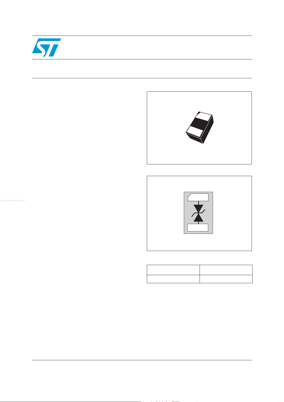
ESDALC6V1-1BM2
SOD-882
■ 1 line low capacitance TRANSIL diode
■ Bidirectional ESD protection
■ Breakdown Voltage V
■ Low diode capacitance (22 pF typ. at 0 V)
■ Low leakage current: < 100 nA at 3 V
■ Very small PCB area: 0.6 mm
Leadfree package
■
= 6.1 V min.
BR
2
Description
The ESDALC6V1-1BM2 is a bidirectional single
line TVS diode designed to protect the datalines
or other I/O ports against ESD transients.
The device is ideal for applications where both
reduced line capacitance and board space saving
are required.
Benefits
■ High ESD protection level
■ High integration
■ Suitable for high density boards
Functional diagram
I/O1
I/O2
Order code
Part number Marking
ESDALC6V1-1BM2 P
Complies with the following standards:
IEC 61000-4-2 level 4
15 kV (air discharge)
8 kV (contact discharge)
TM: TRANSIL is a trademark of STMicroelectronics
MIL STD 883E - Method 3015-7: class 3
HBM (Human body model)
January 2007 Rev 1 1/7
www.st.com
Characteristics ESDALC6V1-1BM2
1 Characteristics
Table 1. Absolute maximum ratings (T
Symbol Parameter Value Unit
(1)
V
PP
P
PP
I
PP
T
T
stg
T
T
OP
1. For a surge greater than the maximum values, the diode will fail in short-circuit.
Table 2. Electrical characteristics (T
Symbol Parameter
Peak pulse voltage (IEC 61000-4-2 contact discharge) ± 30 kV
(1)
Peak pulse power dissipation (8/20 µs) Tj initial = T
Repetitive peak pulse current (8/20 µs) 9 A
Junction temperature 125 °C
j
Storage temperature range - 55 to + 150 °C
Maximum lead temperature for soldering during 10 s 260 °C
L
Operating temperature range - 40 to + 125 °C
amb
amb
= 25° C)
= 25° C)
amb
140 W
I
V
RM
V
V
I
RM
I
PP
V
Part Number
BR
CL
Stand-of voltage
Breakdown voltage
Clamping voltage
Leakage current @ V
Peak pulse current
Forward voltage drop
F
I
R
RM
I
RM
I
RM
I
R
R
d
VRMV
αT
V
BR
C@0V
Bias
V
RM
BR
@ I
VBRV
R
IRM @ V
RM
min. max. max. typ. max. typ.
VVmAnAVΩ 10
-4
/°C pF
ESDALC6V1-1BM2 6.1 8.0 1 100 3 0.65 2.5 22
2/7
ESDALC6V1-1BM2 Characteristics
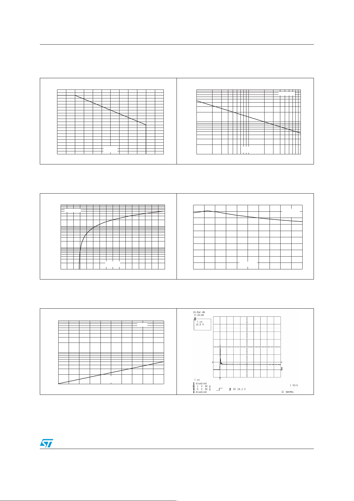
Figure 1. Relative variation of peak pulse
power versus initial junction
temperature
P [T initial] / P [T initial=25°C)
PP j PP j
1.1
1.0
0.9
0.8
0.7
0.6
0.5
0.4
0.3
0.2
0.1
0.0
0 25 50 75 100 125 150
T (°C)
j
Figure 3. Clamping voltage versus peak
pulse current (typical values)
I (A)
PP
100.0
T initial=25°C
j
10.0
Figure 2. Peak pulse power versus
exponential pulse duration
P (W)
PP
1000
100
t (µs)
10
1 10 100
p
T initial=25°C
j
Figure 4. Junction capacitance versus
reverse voltage applied (typical
values)
C(pF)
25
20
15
F=1MHz
V =30mV
OSC RMS
T=25°C
j
1.0
V (V)
0.1
0 5 10 15 20 25 30 35 40
CL
Figure 5. Relative variation of leakage
current versus junction
temperature (typical values)
I [T ] / I [T =25°C]
Rj Rj
100
10
T (°C)
1
25 50 75 100 125 150
j
V =3V
R
10
5
V (V)
0
012345
LINE
Figure 6. ESD response to IEC 61000-4-2
(+15 kV air discharge) on each
channel
3/7
 Loading...