

APPLICATION NOTE
CIRCUITS FOR POWER FACTOR CORRECTION
WITH REGARDS TO MAINS FILTERING
by J. M. Bourgeois
1. INTRODUCTION
The new European Norms EN 60555 and the
international standard IEC555 will impose a limit on
the harmonic content of the input current of mains
supplied equipment. In practice this will require the
addition of a Power Factor Corrector (PFC) at the
input of many types of mains operated electronic
equipment, for example electronic lamp ballasts, TV
power supplies and motor drives. A correctly
designed PFC draws a sinusoidal input current from
the mains supply, in phase with the mains voltage,
and meets the EN60555 norm. It may also provide
additional functions, such as automatic mains voltage
selection and a regulation of the voltage supplied to
the attached equipment.
Size and cost optimization of PFCs must include the
RFI filter on the input, which prevents interference
being fed back to the mains. The addition of the PFC
represents another switching stage in the system,
meaning that larger amount of high frequency noise
is applied to the mains than with a conventional
rectifier/capacitor front end, and so additional RFI
filtering is required. The amount of fitering needed
can be minimized by choosing suitable modulation
techniques and mode of operation of the PFC.
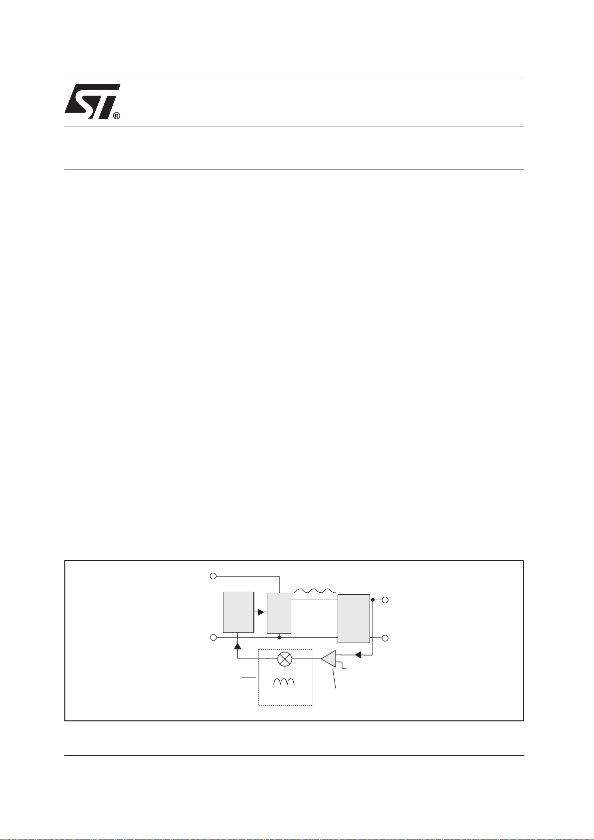
1.1 Basic principles of operation
A power factor corrector is basically a AC to DC
converter, and is usually based on an SMPS
structure. The basic functional blocks of a Power
Factor Corrector are shown in figure 1.
A standard SMPS uses Pulse Width Modulation
(PWM) to adjust the amount of power it supplies to
the attached equipment. The Pulse Width Modulator
controls the power switch, which chops the dc input
voltage into a train of pulses. This train of pulses is
then smoothed, producing the dc output voltage.
This output voltage is then compared with a voltage
reference representing the voltage desired by the
equipment being supplied, and the resulting voltage
difference (the error voltage) is fed back to the input
of the PWM, which varies the width of the pulses it
supplies accordingly - if the output voltage is too
high, the pulse width is reduced, and thus less power
is supplied, and vice versa.
A PFC also uses this method, but adds a further
element to ensure that the current it draws from the
mains is sinusoidal, and remains in phase with the
mains voltage. The error voltage is modulated with a
signal derived from the rectified AC mains, before
Figure 1. Block diagram of a Power Factor Corrector (PFC)
RECTIFIED
AC MAINS
SECTION ADDED
TO STANDARD SMPS
TOPOLOGY
PWM
Chop
Signal derived
from AC mains
Smooth
Reference
voltage
Error amplifier
SMOOTH
DC
OUTPUT
1/9AN510/0894
APPLICATION NOTE
being fed to the PWM input. This means that the
width of the power pulse supplied to the output
device depends both on the basic error voltage and
also on the instantaneous value of the mains voltage.
The PFC thus draws more power from the mains
when the level of the mains voltage is high, and less
when it is low, which results in a reduction of the
harmonics in the drawn current.
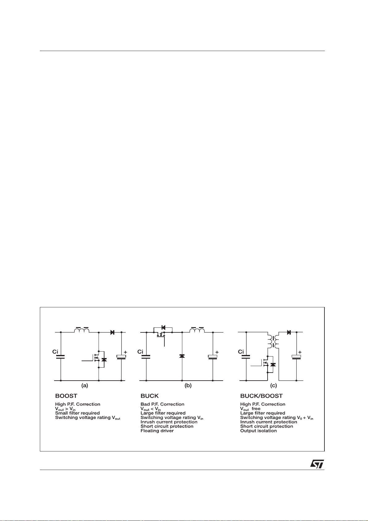
2. ACTIVE POWER FACTOR CORRECTOR
TOPOLOGIES
Among the topologies shown in figure 2, the boost
configuration operating in a continuous current mode
(ie the value of the inductor at the input is calculated
such that it conducts continuously throughout the
switching cycle) applies the smallest amount of high
frequency current to the input capacitor Ci. It is the
only topology which allows the noise across the
input capacitor to be reduced, which is the major
factor defining the size and cost of the filter.
Additionally, the boost inductor stores only a part of
the transferred energy (because the mains still
supplies energy during the inductor demagnetization)
and so the inductor required is smaller in comparison
with the other topologies.
The boost topology thus leads to the cheapest PFC
solution, but does not provide either in-rush current
or short circuit protection. The buck/boost topology
can also be used; its advantages are that it can
provide output isolation and adjustable output voltage.
This paper will take the cost as the most important
consideration, and so will concentrate on the boost
circuit topology.
3. BOOST CIRCUIT PARAMETER OPTIMIZATION
Figure 3 shows the general topology of a boost
PFC. Its optimization requires careful adjustment of
the following parameters:
• the value of the input capacitor C
• the current ripple in boost inductor L
i
b
• the parasitic capacitances of the boost inductor
and the power semiconductors, including those
associated with the heatsink
• the operating frequency and frequency modulation
techniques.
3.1 Value of input capacitor C
i
The noise across the input capacitor, which
determines the cost of the filter, is proportional to the
current ripple and inversely proportional to the
capacitor value.
A value of 3.3µF/kW is a good compromise between
current distortion and noise generation.
3.2 Current ripple in the boost inductor
The current ripple (∆i) is a function of the input
voltage (Vi), output voltage (V
), inductor value
out
(Lb) and switching frequency (fs), and can
Figure 2. Active PFC topologies
2/9
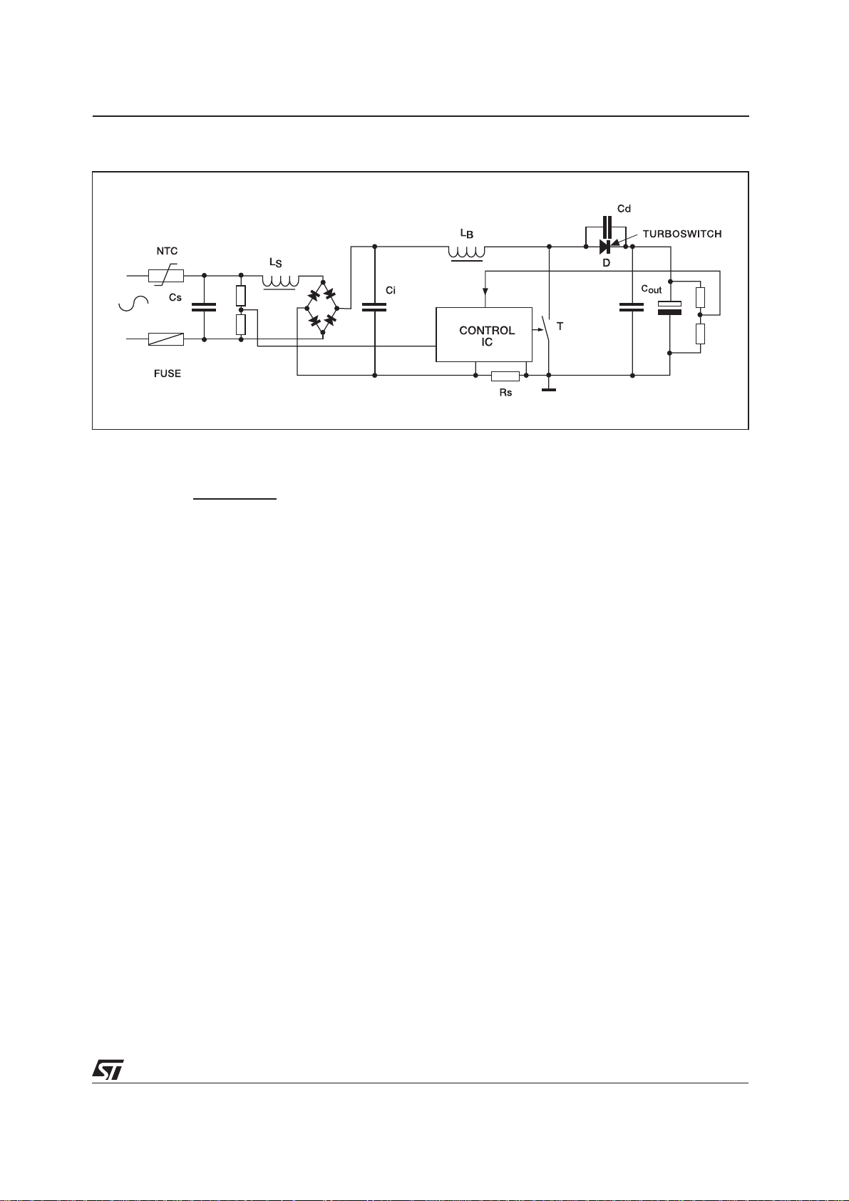
Figure 3. Basic topology of a Boost PFC
APPLICATION NOTE
be expressed as:
(V
- Vi) . V
∆i =
Typical values may be Vi = 300V, V
Fs = 70kHz.
If the system is operating in continuous mode, a
typical value of∆i may be 1A. This means an inductor
value Lb = 1mH.
If instead the system operates in discontinuous mode,
∆i might be 6A, in which case Lb = 150µH.
The inductor current waveforms represented by these
ripple values are shown in figure 4.4.
Using continuous mode requires an inductance value
about ten times that needed when operating in
discontinuous mode; however, the low value of
current ripple means that a cheap and efficient iron
powder core can be used.
When operating with ripple currents larger than
around 1A, the larger dI/dt leads to the occurence of
skin effects and large eddy currents in an iron powder
core, meaning that operation in discontinuous mode
requires a more expensive ferrite core.
As the maximum possible flux density in an iron
powder core is much higher than that in a ferrite core
(around 1.5 Tesla in iron powder against 0.25 in
ferrite), this means that the size (and hence cost) of
inductor required in both cases is around the same.
So, a cheaper system is achieved controlling a small
current ripple by operating in continuous mode,
despite the large inductor value.
out
Fs . Lb . V
out
i
= 400V and
out
3.3 Frequency modulation techniques
The switching frequency used can be constant or
variable. If variable, the switching frequency can be
controlled, or be free to vary within set limits. A
circuit using variable switching frequencies can result
in lower EMI and lower power losses, but the topology
is harder to analyse, and the frequency
characteristics sometimes more difficult to predict.
3.4 Choosing the switching frequency to match
the power semiconductor
When using constant current ripple, increasing the
switching frequency allows a reduction in the value
of the boost inductor. However, increasing the
switching frequency will lead to increased switching
losses in the power semiconductors. In standard
boost PFC circuits, conduction losses in the power
switch will be lower than the switching losses, and
consequently the switching frequency will be limited
by the switching losses of the chosen power
transistor, and the recovery losses of the boost
diode.
Also, if compliance with VFG243 is required, using a
switching frequency below 50kHz (where the
constraints are more relaxed) will lead to a significant
reduction in the cost of the filter.
Power MOSFET transistors are practical and cost
effective in applications using up to 277V AC mains,
with an output power of up to 3kW. The
STE36N50-DK is a perfect solution for applications
in the 1 to 3kW range. This device combines a low
R
DS(on)
Power MOSFET with an ultra-fast
3/9
 Loading...