

ST EMIF10-COM01F2 User Manual
10-line IPAD™, EMI filter including ESD protection
Features
■ EMI symmetrical (I/O) low-pass filter
■ Lead free package
■ Very low PCB space consuming: < 6 mm
■
Very thin package: 0.65 mm
■ High efficiency in ESD suppression on both
input & output pins
■ High reliability offered by monolithic integration
2
EMIF10-COM01F2
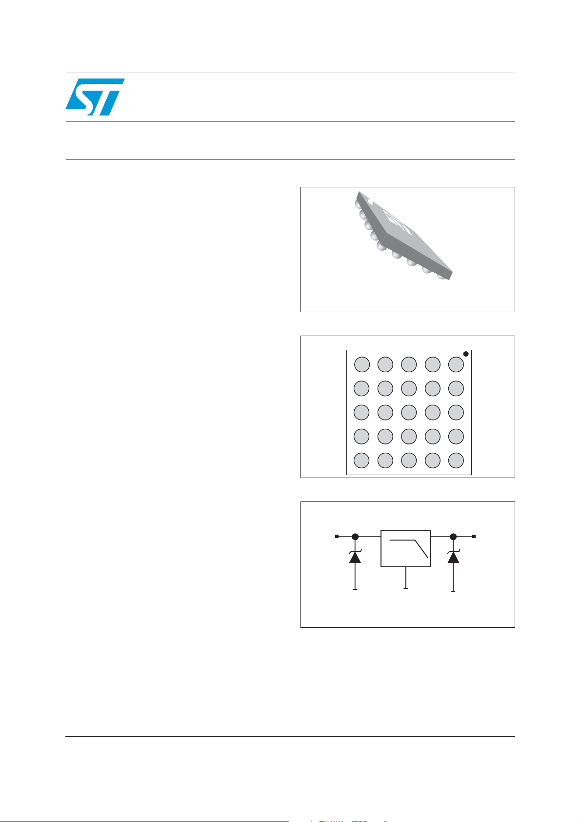
Flip Chip
(25 bumps)
Complies with the following standard:
■ IEC 61000-4-2 level 4
– 15 kV (air discharge)
– 8 kV (contact discharge)
Applications
EMI filtering and ESD protection for:
■ Computers and printers
■ Communication systems
■ Mobile phones
Description
The EMIF10-COM01F2 is a highly integrated
device designed to suppress EMI / RFI noise in all
systems subjected to electromagnetic
interferences. The EMIF10 Flip-Chip packaging
means the package size is equal to the die size.
Additionally, this filter includes an ESD protection
circuitry which prevents damage to the application
when subjected to ESD surges up to 15 kV.
Figure 1. Pin configuration (bump side)
54
I5
3
21
I3
I9 I8I10
GNDGND
I1
I2I4
I6
I7
GNDGND GND
0609 08010 07
0204 0305
01
A
B
C
D
E
Figure 2. Basic cell configuration
Low-pass Filter
Input
R = 200
I/O
C = 45 pF
line
Ω
Output
TM: IPAD is a trademark of STMicroelectronics.
April 2008 Rev 5 1/7
www.st.com
7
Characteristics EMIF10-COM01F2
1 Characteristics
Table 1. Absolute ratings (T
Symbol Parameter and test conditions Value Unit
amb
= 25 °C)
V
T
T
Table 2. Electrical characteristics (T
ESD discharge IEC61000-4-2, air discharge
PP
ESD discharge IEC61000-4-2, contact discharge
Junction temperature 125 °C
T
j
Operating temperature range - 40 to + 85 °C
op
Storage temperature range - 55 to + 150 °C
stg
Symbol Parameter
V
V
V
R
C
Breakdown voltage
BR
I
Leakage current @ V
RM
Stand-off voltage
RM
Clamping voltage
CL
R
Dynamic impedance
d
I
Peak pulse current
PP
Resistance between Input and Output
I/O
Input capacitance per line
line
Symbol Test conditions Min. Typ. Max. Unit
V
BRIR
I
RM
R
R
I/O
C
line
t
LH
= 1 mA 6 8 10 V
VRM = 3 V per line 500 nA
IPP = 10 A, tp = 2.5 µs 1 Ω
d
At 0 V bias 45 50 pF
V
= 2.8 V R
input
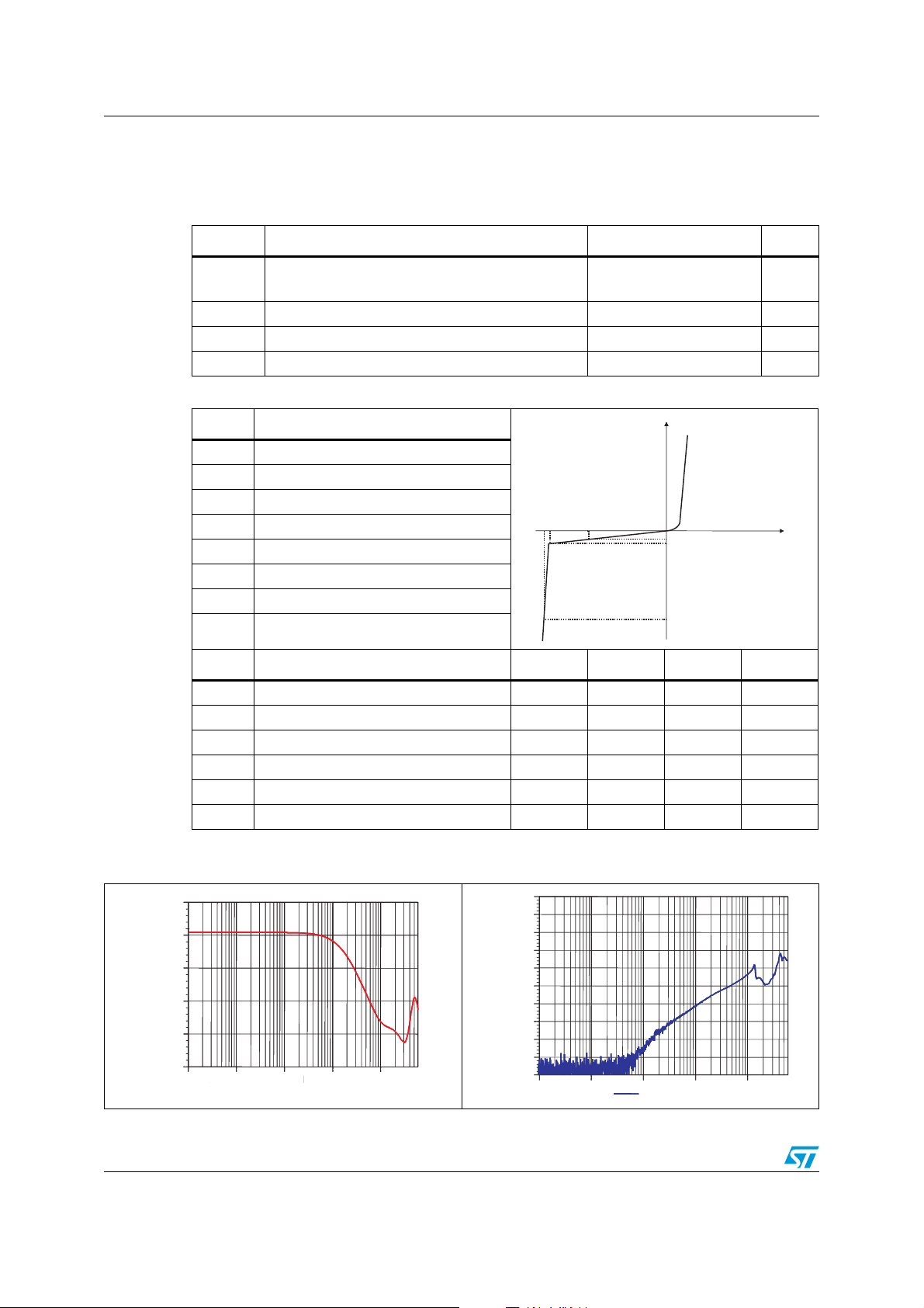
Figure 3. S21(db) attenuation
measurement
0.00
0.00
0.00
dB
dB
dB
-10.00
-10.00
-10.00
-20.00
-20.00
-20.00
-30.00
-30.00
-30.00
-40.00
-40.00
-40.00
-50.00
-50.00
-50.00
100.0k 1.0M 10.0M 100.0M 1.0G
100.0k 1.0M 10.0M 100.0M 1.0G
100.0k 1.0M 10.0M 100.0M 1.0G
(1)
f/Hz
f/Hz
f/Hz
amb
15
8
= 25 °C)
kV
I
RM
V
CL
V
V
RM
BR
slope : 1 / R d
I
RM
I
R
I
PP
V
180 200 220 Ω
= 100 kΩ 25 ns
load
Figure 4. Analog crosstalk
0.00
0.00
dB
dB
-10.00
-10.00
-20.00
-20.00
-30.00
-30.00
-40.00
-40.00
-50.00
-50.00
-60.00
-60.00
-70.00
-70.00
-80.00
-80.00
-90.00
-90.00
-100.00
-100.00
100.0k 1.0M 10.0M 100.0M 1.0G
100.0k 1.0M 10.0M 100.0M 1.0G
Xtalk 1/2
f/Hz
f/Hz
1. Spikes at high frequencies are induced by the PCB layout
2/7
EMIF10-COM01F2 Characteristics
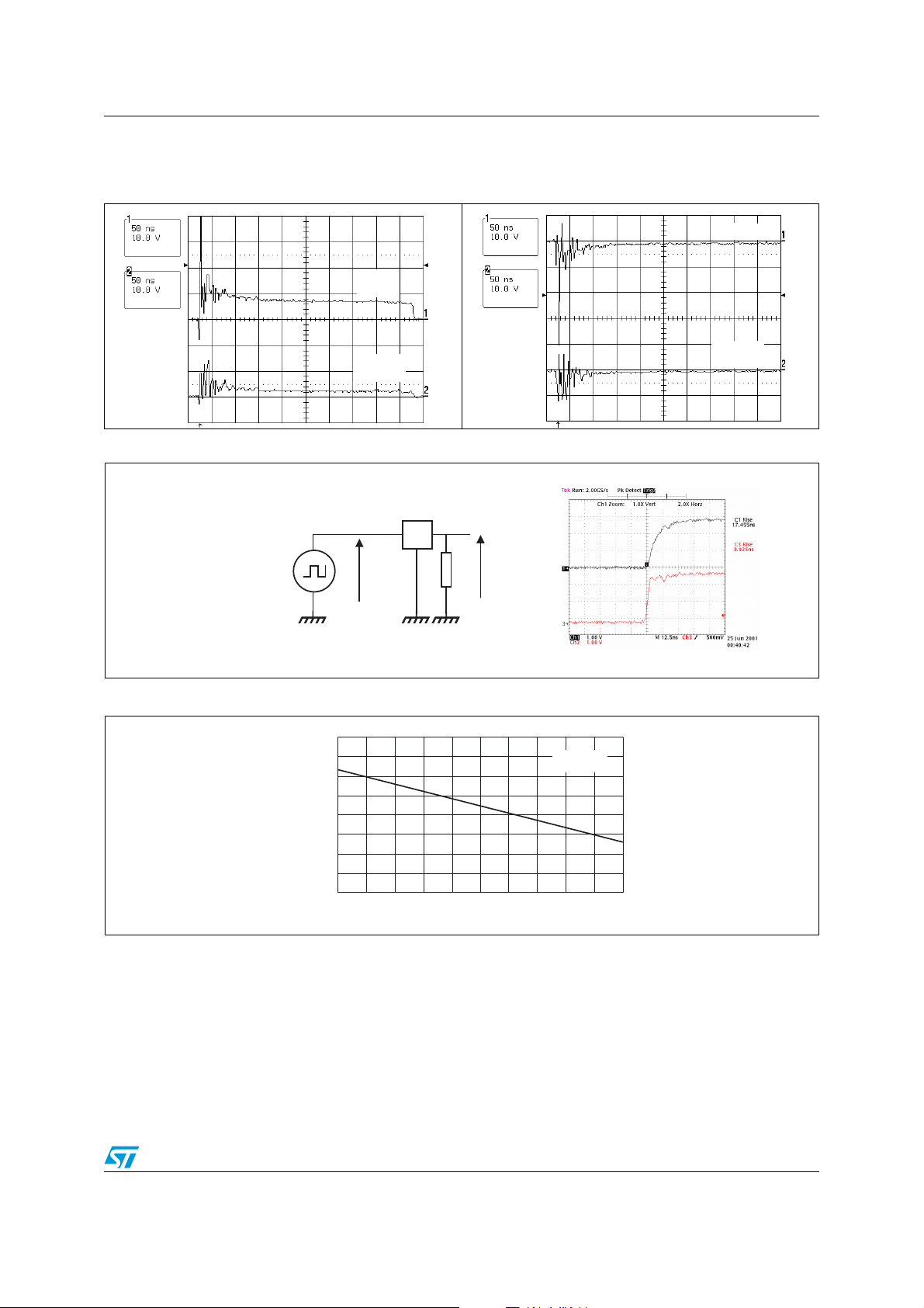
Figure 5. ESD response to IEC 61000-4-2
(+15 kV air discharge) on one input
) and on one output (V
(V
in
V(out1)
V(in1)
out
)
Figure 7. Rise time measurement
EMIF10-COM01F2
In Out
Square signal
Generator Vc = 2.8V
Vin
Figure 6. ESD response to IEC 61000-4-2
(-15 kV air discharge) on one input
100k
(Vin) and on one output (V
Vout
out
V(in1)
V(out1)
)
Figure 8. Capacitance versus reverse applied voltage
C(pF)
50
40
30
20
10
012345
VR(V)
F=1MHz
Vosc=30mV
3/7
 Loading...