

6-line IPAD™, EMI filter and ESD protection for SD card
Features
■ ESD protection (IEC standard)
■ EMI Filtering
■ Level translator
■ Signal conditionning
■ Integrated power supply with:
– Thermal shutdown (TSD)
– Under voltage lockout (UVLO)
– Short-circuit current limitation (I
– Power on/off feature with Enable pin
SC
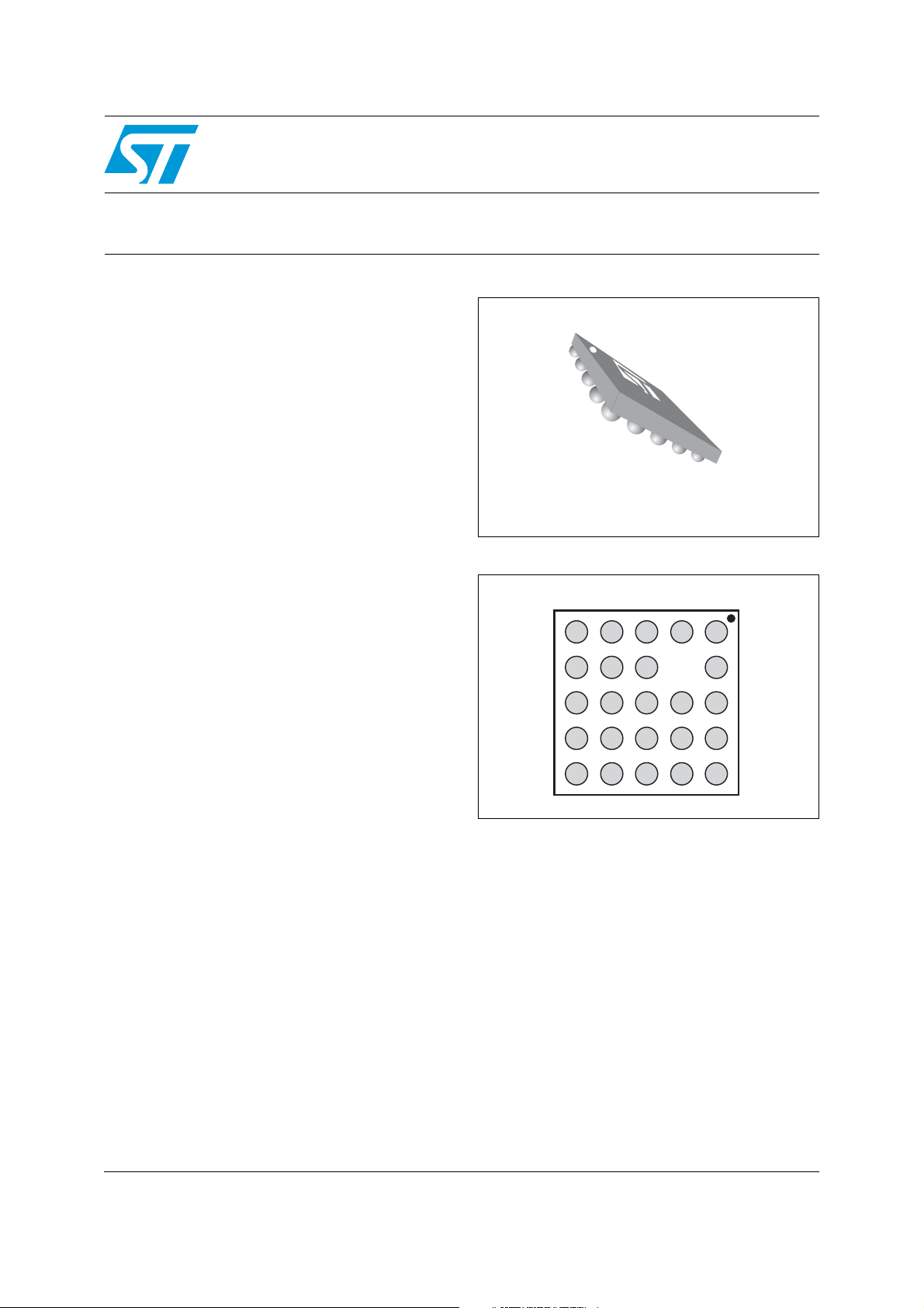
EMIF06-SD03F3
Flip Chip
)
(24 bumps)
Benefits
■ EMI Low-pass-filter and ESD protection (up to
15 kV on external pins)
■ Integrated pull up resistors prevent bus floating
■ 50 MHz clock frequency compatible with
C
< 40 pF
line
■ Lead-free package in 400 µm pitch
■ Low power consumption
■ Very low PCB space consumption
■ High reliability offered by monolithic integration
■ Reduction of parasitic elements thanks to CSP
integration
Complies with the following standards:
■ IEC 61000-4-2, Level 4: External pins
– 15 kV (air discharge)
– 8 kV (contact discharge)
■ HBM IEC 61340-3-1: All pins
– 2 kV (air discharge)
– 2 kV (contact discharge)
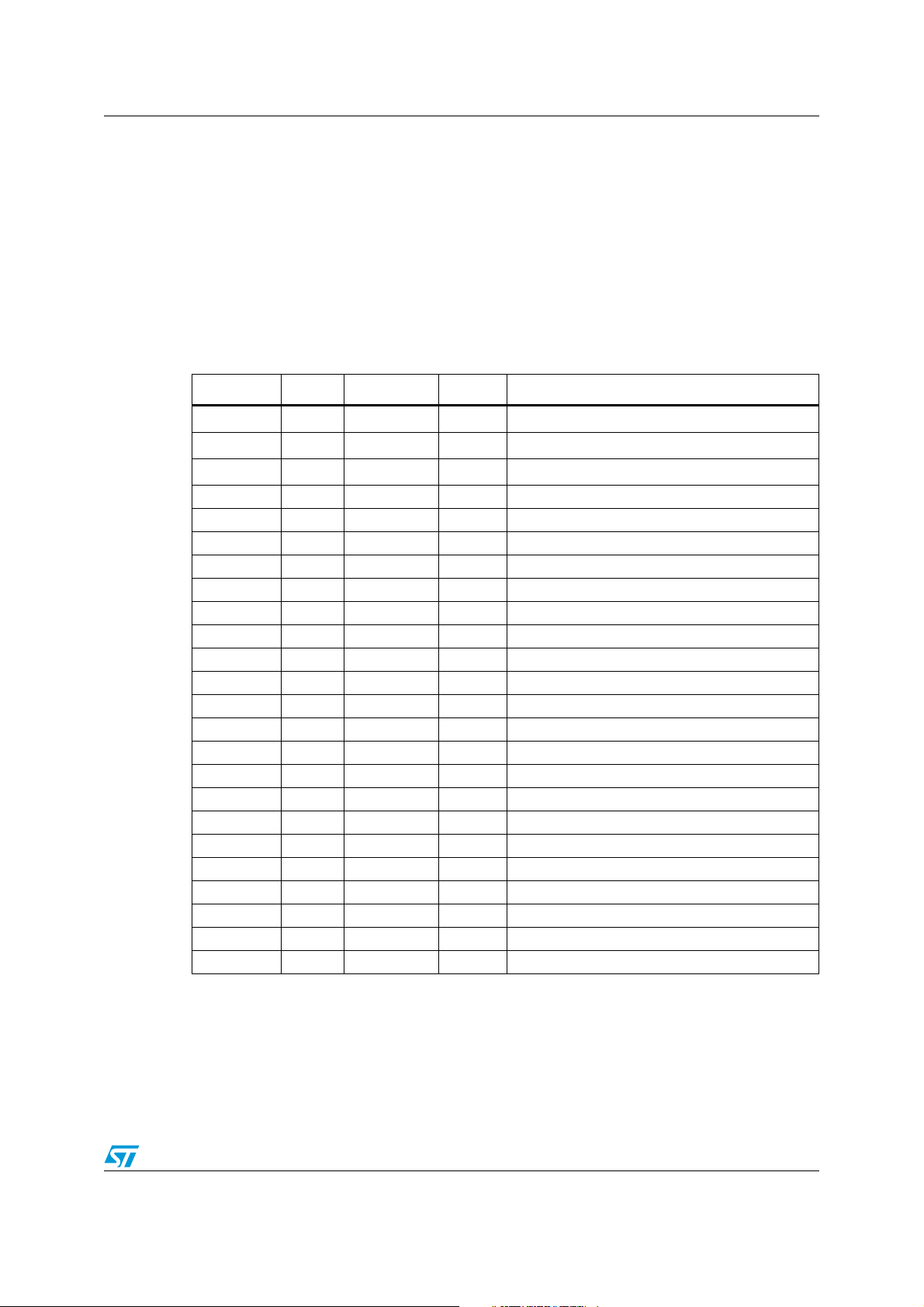
Figure 1. Pin configuration (bump side)
5
3
4
12
A
B
C
D
E
Applications
■ Removable memory cards in mobile phones,
communication systems, and portable
applications
■ Memory cards compliant with: SD (standard
and high speed), MiniSD, µSD and
MMC/Trans-flash standards
Description
The EMIF06-SD03F3 is a highly integrated
device, based on IPAD technology, combining the
TM: IPAD is a trademark of STMicroelectronics.
February 2010 Doc ID 15194 Rev 2 1/23
5 functions described under Features.
www.st.com
23

Contents EMIF06-SD03F3
Contents
1 Functional description . . . . . . . . . . . . . . . . . . . . . . . . . . . . . . . . . . . . . . . 3
2 Characteristics . . . . . . . . . . . . . . . . . . . . . . . . . . . . . . . . . . . . . . . . . . . . . 6
3 Passive integration and low pass filter . . . . . . . . . . . . . . . . . . . . . . . . . . 8
4 Data transmission . . . . . . . . . . . . . . . . . . . . . . . . . . . . . . . . . . . . . . . . . . 10
4.1 Test circuit from host to SD . . . . . . . . . . . . . . . . . . . . . . . . . . . . . . . . . . . 11
4.2 Test circuit from SD to host . . . . . . . . . . . . . . . . . . . . . . . . . . . . . . . . . . . 12
4.3 Measurement of t
4.4 Measurement of t
(host to SD) from rising edge CLK.h . . . . . . . . . . . 12
skew
(read mode) from rising edge CLK.h . . . . . . . . . . 13
skew.f
5 Low drop out voltage regulator . . . . . . . . . . . . . . . . . . . . . . . . . . . . . . . 14
5.1 Line regulation and transient line regulation . . . . . . . . . . . . . . . . . . . . . . . 17
5.2 Load regulation and transient load regulation . . . . . . . . . . . . . . . . . . . . . 18
5.3 Dropout definition . . . . . . . . . . . . . . . . . . . . . . . . . . . . . . . . . . . . . . . . . . . 19
6 Application schematic . . . . . . . . . . . . . . . . . . . . . . . . . . . . . . . . . . . . . . 19
7 Ordering information scheme . . . . . . . . . . . . . . . . . . . . . . . . . . . . . . . . 20
8 Package information . . . . . . . . . . . . . . . . . . . . . . . . . . . . . . . . . . . . . . . . 20
9 Ordering information . . . . . . . . . . . . . . . . . . . . . . . . . . . . . . . . . . . . . . . 21
10 Revision history . . . . . . . . . . . . . . . . . . . . . . . . . . . . . . . . . . . . . . . . . . . 22
2/23 Doc ID 15194 Rev 2
EMIF06-SD03F3 Functional description
1 Functional description
A SIDE (Host-CPU) pin list:
V
, Enable, Dat123.dir, CMD.dir, CMD.h, CLK.h, CLK -f, Dat0.dir, Dat0.h, Dat1.h, Dat2.h,
ccA
Dat3.h, V
B SIDE (SD-Card) pin list:
bat
WP, CD, V
Table 1. Pin definition
, CMD-B, CLK-B, Dat0-B, Dat1-B, Dat2-B, Dat3-B
ccB
Pin name Bump Type Side Description
V
ccA
V
ccB
V
bat
B3 Power input A
B4 Power output B
A4 Power input A
GND C4 Ground - Ground
GND C3 Ground - Ground
Enable C2 Input A Internal power supply enable
CMD.dir A2 Input A Command direction
CMD.h D2 IO A A side command
CLK.h C1 Input A Clock input
CLK-f E2 Output A Clock feedback
Dat0.dir A3 Input A Data direction
Dat0.h D1 IO A Data host
Dat123.dir E3 Input A Data direction
Dat1.h E1 IO A Data host
Dat2.h A1 IO A Data host
Dat3.h B1 IO A Data host
WP E4 Input to CPU A Write protect
CD D3 Input to CPU A Card detect
CMD-B D4 IO B Command direction
CLK-B C5 Output B Clock output
Dat0-B D5 IO B Data SD
Dat1-B E5 IO B Data SD
Dat2-B A5 IO B Data SD
Dat3-B B5 IO B Data SD
Power supply (1.8v)
Power supply (internally generated, 2.9 V)
Battery power supply
Note: In Ta bl e 5 , 6, 7, and 10, collective names are used for groups of pins. The names used are:
*.dir = CMD.dir, Dat0.dir, Dat123.dir
*.h = CMD.h, CLK.h, Dat0.h, Dat1.h, Dat2.h, Dat3.h
*-B = CMD-B, CLK-B, Dat0-B, Dat1-B, Dat2-B, Dat3-B
V
= All A side input pins
iA
V
= All B side input pins.
iB
Doc ID 15194 Rev 2 3/23
Functional description EMIF06-SD03F3
Table 2. Function table
Command signals A side signals direction B side signal direction
Enable CMD. dir Dat0.dir Dat123.dir CMD.h CLK.h CLK-f Dat0.h
Dat1.h
Dat2.h
Dat3.h
CMD-B CLK-B Dat0-B
Dat1-B
Dat2-B
Dat3-B
H H X X IN IN OUT X X OUT OUT X X
H L X X OUT IN OUT X X IN OUT X X
H X H X X IN OUT IN X X OUT OUT X
H X L X X IN OUT OUT X X OUT IN X
HX X HXINOUTXINXOUTXOUT
H X X L X IN OUT X OUT X OUT X IN
L X X X X X Z X X L* Z L* L*
Note: 1 When A side signals direction is INPUT, SD-CARD is WRITTEN by CPU-Host (i.e B side
signals direction is OUTPUT)
When A side signals direction is OUTPUT, SD-CARD is READ by CPU-Host (i.e B side
signals direction is INPUT)
2 For B side signals when Enable = L:
* Defined by internal pull-down (see Figure 3 for pins CMD.B and data bus Dat[0…3].B)
Figure 2. Configuration
CPU
Feedback Clk
CMD
CMD Dir
Dir0
Dir1-3
WP, CD
VccA 1.8 V
ESD
2 kV
Vbat
IPAD
Low drop out
voltage regulator
Clk Clk
CMD CMD
Data 0 - 3 Data 0 - 3
ESD (15 kV)
and EMI
VccB
Mini
SD
4/23 Doc ID 15194 Rev 2
EMIF06-SD03F3 Functional description
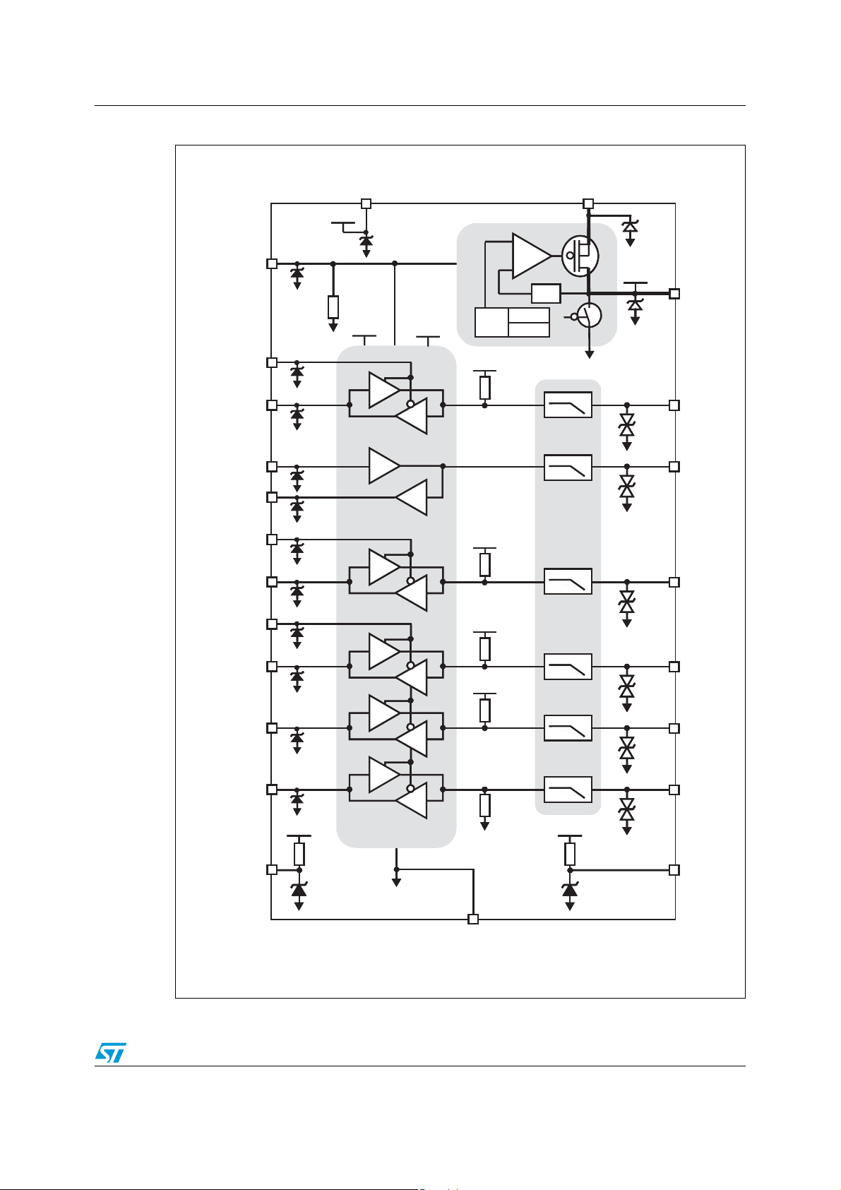
Figure 3. Block diagram
Enable
Enable
Enable
Enable
EnableEnable
CMD.dir
CMD.h
CLK.h
CLK-f
Dat0.dir
Dat0.h
Dat123.dir
Dat1.h
Dat2.h
2KV
2KV
2KV2KV
2KV
2 kV
500KW
500KW
500KW500KW
500KW
500 k Ω
2KV
2KV
2KV
2KV
2 kV
2KV
2KV
2KV
2KV
2 kV
2KV
2KV
2KV
2KV
2 kV
2KV
2KV
2KV
2KV
2 kV
2KV
2KV
2KV
2KV
2 kV
2KV
2KV
2KV
2KV
2 kV
2KV
2KV
2KV
2KV
2 kV
2KV
2KV
2KV
2KV
2 kV
2KV
2KV
2KV
2KV
2 kV
VCCA
VCCA
VCCAVCCA
VCCA
V
ccA
R
V
ccA
EN
V
VCCA
VCCAVCCA
VCCA
ccA
2KV
2KV
2KV2KV
2KV
2 kV
V
VCCB
VCCBVCCB
VCCB
ccB
R9
R10
R11
V
REF
VREF
VREF
VREF
VREF
REF
REF
REF
REF
REF
REF
V
VCCB
VCCB
VCCB
VCCBVCCBVCCB
VCCB
ccB
V
VCCB
VCCB
VCCB
VCCBVCCBVCCB
VCCB
ccB
V
VCCB
VCCB
VCCB
VCCBVCCBVCCB
VCCB
ccB
V
ccB
VCCB
VCCB
VCCB
VCCBVCCBVCCB
VCCB
15KW
15KW
15KW
15KW
15KW
15 k Ω
70KW
70KW
70KW
70KW
70KW
70KW
70KW
70KW
70KW
70KW
70 k Ω
70KW
70KW
70KW
70KW
70KW
70 kR12
A
A
A
A
A
A
OTP
OTP
OTP
OTP
OTP
OTP
UVLO
UVLO
UVLO
UVLO
UVLO
UVLO
Ω70 k
Ω
LDO
LDO
LDO
LDO
R,C
R,C
R,C
R,C
R,C
R,C
Filters
Filters
Filters
Filters
FiltersFilters
EMI
EMI
EMI
EMI
EMI
V
bat
15KV
15KV15KV15KV15KV
15KV
2 kV
VCCB
VCCB
VCCBVCCB
VCCB
V
ccB
V
15KV
15KV
15KV
15KV
15 kV
15KV
ccB
CMD-B
15KV
15 kV
15KV
15KV
15KV
15KV
CLK-B
15KV
15KV
15KV
15KV
15KV
15 kV
Dat0-B
15KV
15 kV
15KV
15KV
15KV
15KV
Dat1-B
-
-
-
-
-
15KV
15 kV
15KV
15KV
15KV
15KV
Dat2-B
15KV
15 kV
15KV
15KV
15KV
15KV
Dat3.h
R14
V
VCCA
VCCA
VCCA
VCCAVCCA
VCCA
ccA
2KV
2KV
2KV
2KV
2kV
100KW
100KW
100KW
100KW
100KW
100k
Level-Shifters
Level-ShiftersLevel-Shifters
Level-Shifters
Level-shifters-
Ω
470KW
470KW
470KW470KW
470KW
470kR7 Ω
V
VCCA
VCCA
VCCA
VCCAVCCAVCCA
VCCA
ccA
100KW
100KW
100KW
100KW
100KW
100 kR13 Ω
15KV
15KV
15KV15KV
15KV
15 kV
Dat3CD-B
WP
15KV
15KV
15KV
15KV
15KV
15kV
EMIF06--
EMIF06--
EMIF06--
EMIF06
EMIF06
EMIF06
EMIF06-
SD02F3
SD02F3
SD02F3
SD02F3
SD03F3
GND
15KV
15KV
15KV
15KV
15KV
15 kV
Doc ID 15194 Rev 2 5/23
Characteristics EMIF06-SD03F3
2 Characteristics
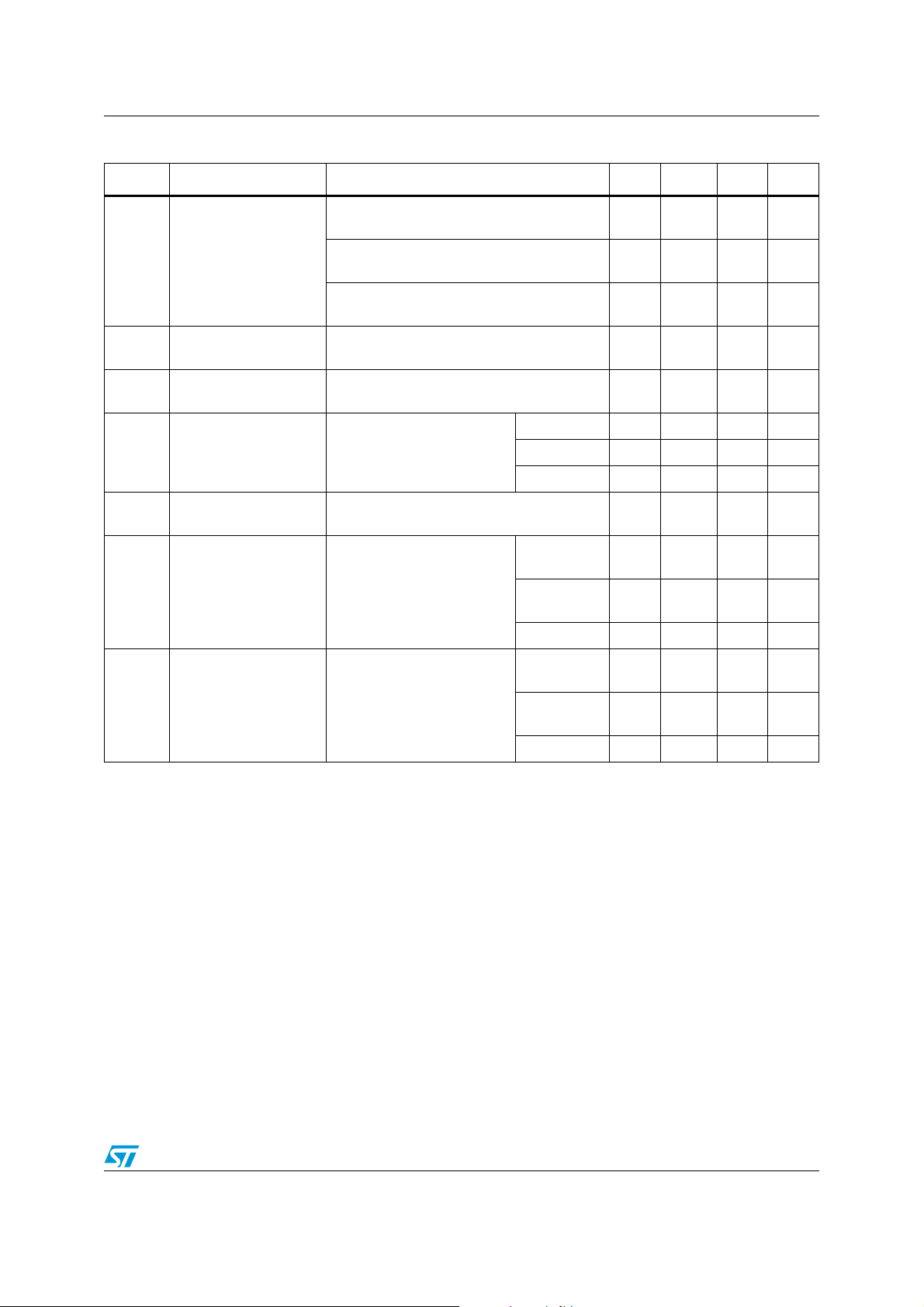
Table 3. Absolute maximum ratings
Symbol Parameter Value Unit
A SIDE (Host-CPU)
All pins: HBM IEC61340-3-1
, Enable, Dat123.dir, CMD.dir, CMD.h, CLK.h,
V
ccA
CLK -f, Dat0.dir, Dat0.h, Dat1.h, Dat2.h, Dat3.h, V
bat
Air discharge
Contact discharge
2
2
ESD
B SIDE (SD-Card)
External pins : IEC 61000-4-2, level 4
, CMD-B, CLK-B, Dat0-B, Dat1-B, Dat2-B,
V
ccB
Dat3-B, WP, CD
Maximum junction temperature 150 °C
Thermal resistance from junction to ambient
(1)
Board: Epoxy FR4, copper thickness = 40 µm, 4 layers
Maximum power dissipation:
P
= (T
dmax
Storage temperature range -55 to +150 °C
stg
V
, V
bat
- T
jmax
, Enable -0.3 to 5.5V
ccB
aopmax
)/ Rth (j-a)
R
th (j-a)
T
P
jmax
dmax
T
CMD-B, CLK-B, Dat0-B, Dat1-B, Dat2-B, Dat3-B -0.3 to V
Voltage
V
ccA
Dat123.dir, CMD.dir, CMD.h, CLK.h, CLK -f, Dat0.dir, Dat0.h, Dat1.h, Dat2.h,
Dat3.h, WP, CD
1. V
is an internally generated power supply, no external voltage should be applied on this pin other than a current clamp.
ccB
The thermal resistance depends on printed circuit board layout. To dissipate the heat efficiently away from Flip Chip bumps,
it is better to make copper planes the largest possible as well as considering thermal vias usage.
Air discharge
Contact discharge
-0.3 to 3.3
-0.3 to V
15
8
64
1W
+ 0.3
ccB
+0.3
ccA
kV
°C/
W
V
6/23 Doc ID 15194 Rev 2
EMIF06-SD03F3 Characteristics
Table 4. Recommended operating conditions
Symbol Parameter Conditions Min. Typ. Max. Unit
V
ccA
V
bat
I
out
C
bat
(1)
C
out
(2)
ESR
T
aop
T
jop
P
dop
Enable Enable input voltage 0 - V
Power supply 1.62 1.8 1.92 V
Battery power supply 3.1 - 5 V
V
output current 0.10 100 200 mA
ccB
External battery
capacitance
External output
capacitance
Equivalent series
resistance for C
out
Ceramic capacitor - 2.20 - µF
= -40 °C to +85 °C, V
T
a
Multi-layer ceramic capacitor type like:
C20RX7R1C225K
= 0 V to 3.3 V
bias
1.4
(-35%)
2.20
3.0
(+35%)
F = 1 Hz to 10 MHz
Multi-layer ceramic capacitor type like:
-3200mΩ
C2012X7R1C225KT
Ambient operating temperature -30 25 85 °C
Juntion operating temperature -30 25 125 °C
Maximum power
dissipation
P
= (T
- T
dop
jop
aop
)/R
th (j-a)
--625mW
ccA
External
pins (without
CMD-B, CLK-B, Dat0-B, Dat1-B, Dat2-B, Dat3-B 0 - V
ccB
WP and CD)
Internal pins
(except
Enable, with
WP, CD, Dat123.dir, CMD.dir, CMD.h, CLK.h,
CLK-f, Dat0.dir, Dat0.h, Dat1.h, Dat2.h, Dat3.h
0-V
ccA
WP and CD)
1. C
= 2.2 µF is minimum allowable capacitance value to guarantee LDO stability
out
2. Values for ESR include the V
minimized in PCB design.
ccB
resistance path and C
- C
out
- GND resistance path. These resistance paths need to be
out
µF
V
V
V
Doc ID 15194 Rev 2 7/23
Passive integration and low pass filter EMIF06-SD03F3
Table 5. LDO - current levels in recommended operating conditions
Symbol Parameter Test conditions
I
Q_OFF
I
Q_ON
Quiescent current consumption
I
_OFF
ccA
Quiescent current consumption
I
_OFF
bat
Quiescent current consumption
(Ground pin current) I
bat
+ I
ccA
(1)
VEN = 0.4 V, V
= 3.4 V, V
bat
= 1.92 V
ccA
*.dir, *.h, *-B = GND, WP = CD = V
All other pins floating
VEN = 0.4 V, V
= 5 V, V
bat
= 1.92 V
ccA
*.dir, *.h, *-B = GND
All other pins floating
I
Level shifter disactivated
ccA
bat
= V
= 3.4 V
= 1.8 V
CLK.h
*.dir = 0 V, V
VEN = V
All other pins floating
out
I
out
I
out
I
out
Min. Typ. Max. Unit
ccA
= 100 µA - 160 220 µA
= 50 mA - 320 375 µA
= 100 mA - 470 550 µA
= 200 mA - 750 900 µA
1. See Note: on page 3 for definition of collective names of pins, for example *.dir
Table 6. Level shifter - current levels in recommended operating conditions
Symbol Parameter Test conditions
I
_ON
ccA
I
_ON
ccB
Quiescent current on V
Quiescent current on V
ccA
ccB
VEN = V
*.dir = V
VEN = V
ccA
ccA
ccA
*.dir = 0 V, V
= 1.92 V, V
bat
, ViA = *.h = V
= 1.92 V, V
ccB
bat
= 3.05 V, ViB = V
(1)
= 3.4 V
ccA
= 3.4 V
ccB
Min. Typ. Max. Unit
-310µA
-1530µA
1. See Note: on page 3 for definition of collective names of pins, for example *.dir
--1µA
--1µA
3 Passive integration and low pass filter
Figure 4. Circuit diagram of EMIF06-SD03F3 (without LDO)
R10
level
Host side
VccA
CLK.h
CMD.h
Data0.h
Data1.h
Data2.h
Data3.h
R14
R13
Enable
WP
CD
ESD 15 kV
Shifter
ESD
2 kV
EN
R
Note: VBR in 14 V technology for pins: CMD-B, CLK-B, Dat0-B, Dat1-B, Dat2-B, Dat3-B, WP, CD
in 8 V technology for pins: Vcc-B, CLK.h, CLK-f, CMD.h, Dat0.h, Dat1.h, Dat2.h, Dat3.h
V
BR
R12
R9
R11
R1
R2
R3
R4
R5
R6
R7
GND
GND
GND
GND
Card side
CLK B
CMD B
Data0 B
Data1 B
Data2 B
Data3 B
ESD 15 kV
15 kV
VccB
15 kV15 kV15 kV
8/23 Doc ID 15194 Rev 2

EMIF06-SD03F3 Passive integration and low pass filter
Table 7. Components
Symbol Parameter Test conditions
= 3.4 V, *.dir = V
C
in-A
C
in-B
C
EMIF
R1, R2, R3, R4,
R5, R6
R
line
Input capacitance for A
side
Input capacitance for B
side
Capacitance seen on B side from EMIF filter - 15 - pF
EMIF resistors
(2)
Line resistance at 20 mA 40 50 60 Ω
R10, R11, R12 EMIF resistors
R9 EMIF resistor
R7 EMIF resistor
R13 EMIF resistor
R14 EMIF resistor
R
EN
resistor
(4)
(3)
(4)
(4)
(4)
(4)
(4)
V
bat
F = 1 MHz, Vdc = 0 V, ±30 mV, VAC = 30mV
= 3.4 V, *.dir = GND, V
V
bat
F = 1 MHz, Vdc = 0 V, ±30 mV, VAC = 30mV
Tj = 25 °C - 40 - Ω
Tj = 25 °C 49 70 91 kΩ
Tj = 25 °C 10.5 15 19.5 kΩ
Tj = 25 °C 329 470 611 kΩ
Tj = 25 °C 70 100 130 kΩ
Tj = 25 °C 70 100 130 kΩ
Tj = 25 °C - 500 - kΩ
1. See Note: on page 3 for definition of collective names of pins, for example *.dir
2. These values are guaranteed by design and statistical process control.
3. 20% tolerance in resistance value
4. 30% tolerance in resistance value
Figure 5. Frequency response with level
shifters internally bypassed
(1)
Figure 6. Crosstalk response with level
EN
= V
ccA
EN
(1)
Min. Typ. Max. Unit
-510pF
= V
ccA
-2535pF
shifters internally bypassed
(1)
dB
0.00
- 5.00
- 10.00
- 15.00
- 20.00
- 25.00
- 30.00
100.0k 1.0M 10.0M 100.0M 1.0G
a1- a5
c1 - c5 d1- d5
e1- e5
1. Measurement in 50 Ω environment
F (Hz)
f/Hz
b1- b5
dB
0.00
- 20.00
- 40.00
- 60.00
- 80.00
- 100.00
F (Hz)
- 120.00
100.0k 1.0M 10.0M 100.0M 1.0G
a1- b5 c1 - d5
d1- e5
Doc ID 15194 Rev 2 9/23

Data transmission EMIF06-SD03F3
4 Data transmission
All values in the tables below are guaranteed across the operating temperature and voltage
range unless otherwise specified.
Table 8. DC voltage levels on host side
Symbol Parameter
V
IHA
V
ILA
V
OHA
V
OLA
Table 9. DC voltage levels on SD side
High level input voltage 0.65 x V
Low level input voltage 0 0 0.35 x V
High level output
voltage
Low level output voltage Iol = 7 mA - 0 0.45 V
Symbol Parameter
V
V
V
OHB
V
OLB
1. V
Table 10. DC current levels
High level input voltage 0.7 x V
IHB
Low level input voltage - 0 0.3 x V
ILB
High level output voltage Ioh = -8 mA V
Low voltage output voltage Iol = 8 mA - 0 0.7 V
is defined in power supply block.
ccB
Symbol Parameter Test conditions
I
I
LSD
I
SCH
I
SCSD
1. See Note: on page 3 for definition of collective names of pins, for example *.dir
Leakage current on
LH
host pin
Leakage current on
SD pin
Short circuit current
on host side
Short circuit current
on SD side
VEN = *.dir = V
ViA = V
V
bat
V
CMD
V
Dat3
SD input = H, host= 0 V
SD input = 0 V, host = V
*.dir = 0 V, V
Host input = H, SD = 0 V
Host input= L, SD = V
*.dir = V
Tes t
conditions
I
= -6 mA V
oh
Tes t
conditions
ccA
or GND, V
ccA
= 3.4 V, V
= V
Dat0
CLK.h
= V
= *.dir = GND
= 3.4 V, Tj = 25 °C
bat
= 1.8 V, V
ccA
ccA
= 1.92 V,
= 3.4 V
bat
= V
ccA
= V
Dat1
ccA
ccB
= 3.4 V
bat
Min. Typ. Max. Unit
ccA
- 0.45 - - V
Min. Typ. Max. Unit
(1)
ccB
(1)
- 0.7 2.9 - V
ccB
(1)
,
= V
Dat2
ccB
= 1.8 V
, Tj = 25 °C
V
ccA
V
ccB
-V
ccA
-V
ccB
Min. Typ. Max. Unit
--5µA
--5µA
-25 -mA
-60 -mA
(1)
V
V
10/23 Doc ID 15194 Rev 2
EMIF06-SD03F3 Data transmission
Figure 7. Symbol definitions of t
INPUT
t
plh
70%
OUTPUT
Table 11. AC characteristics
20%
50%
t
r
(1)
, t
plh
, tr and tf for AC characteristics in Tab l e 11
phl
VorV
t
f
0V
50%
20%
ccA ccB
VorV
ccA ccB
0V
50%50%
t
phl
70%
Symbol Parameter Test conditions Min. Typ. Max. Unit
t
t
t
t
Propagation delay hl from host to SD
phl
Propagation delay lh from host to SD - 3.5 6
plh
Propagation delay hl from SD to host
phl
Propagation delay lh from SD to host - 3 6
plh
Section 4.1
Section 4.2
-3.56
-36
Rise time from host to SD Section 4.1 -1.53
t
r
Rise time from SD to host Section 4.2 -0.52
Fall time from host to SD Section 4.1 -1.93
t
f
Fall time from SD to host Section 4.2 -0.52
t
skew
t
skew.ftskew
t
p_clkf
t
r_clkf
t
f_clkf
1. T
Delay differences from host to SD Section 4.1,Section 4.3 -1.0 0 1.0 ns
delay from SD to host Section 4.2, Section 4.4 -1.5 0 1.5 ns
Propagation delay for CLK feedback - 6.5 12 ns
Rise time for CLK feedback Section 4.2 -0.52 ns
Fall time for CLK feedback Section 4.2 -0.52 ns
-30 to 85 °C, I
aop
= 1 mA, C
out
= 2.2 µF, C
bat
= 2.2 µF
out
ns
ns
ns
ns
4.1 Test circuit from host to SD
Test circuit from host to SD is shown in Figure 8. Timings are measured for the whole line
cell (shifter + EMI + ESD) on an external load C
card capacitance 10 pF).
Figure 8. Test circuit from host to SD
= 15 pF (board capacitance 5 pF + SD
sd
HOST
SD
Csd=15 pF
Doc ID 15194 Rev 2 11/23

Data transmission EMIF06-SD03F3
4.2 Test circuit from SD to host
Test circuit from SD to host is shown in Figure 9. Timings are measured for the whole line
cell (shifter + EMI + ESD) on an external load C
capacitance).
Figure 9. Test circuit from SD to host
= 5 pF (board capacitance + host
host
C
4.3 Measurement of t
Figure 10. Example of measurement of t
50%
50%
= 5 pF
host
skew
CPU
CPU
t
= Tp(CLK.h
skew
50%
50%
HOST
SD
(host to SD) from rising edge CLK.h
(host to SD) from rising edge of CLK.h
skew
CLK-B
CLK.h
CLK.f
DAT.dir
DAT.h
= « 1 »
= « 1 »
Tp(Datx.h
Tp(CLK.h
CLK
Datx
CLK
EMIF06-SD02F3
EMIF06-SD03F3
-
B)
-
B)
-
B)
CLK-B
Dat-B
- Tp(Datx.h
15pF
15pF15pF
15pF
15pF15pF
MiniSD card
MiniSD card
Datx
V
ccA
0V
V
ccB
0V
V
ccA
0V
V
ccB
0V
-
B)
Dat.h
Dat
x-
CLK.h
CLK
B
-
B
12/23 Doc ID 15194 Rev 2

EMIF06-SD03F3 Data transmission
4.4 Measurement of t
Figure 11. Example of measurement of t
CPU
skew.f
=
Tp (
CLK.h
50%
t
skew.f
CLK.h
CLK.f
DAT.dir
5pF
DAT.h
5pF
50%
50%
(read mode) from rising edge CLK.h
for read mode from rising edge of CLK.h
skew.f
Datx.h.h)
CLK-B
15pF
Dat-B
MiniSD card
V
ccA
CLK.
h
0V
V
ccB
CLK
0V
V
ccB
Datx-B
0V
V
ccA
Datx
)
f
0V
V
ccA
CLK.
0V
f
CLK.
50%
delay
= « 0 »
EMIF06-SD03F3
)
f
–[Tp(CLK.h CLK-B) + Tp(Datx-B Datx.h)]
Tp(CLK.h
50%
CLK--BB)
Tp(Datx-B
Tp (
CLK.h
CLK.
Datx.h = Dat0.h, Dat1.h, Dat2.h, Dat3.h, CMD.h
Datx-B = Dat0-B, Dat1-B, Dat2-B, Dat3-B, CMD.B
Doc ID 15194 Rev 2 13/23

Low drop out voltage regulator EMIF06-SD03F3
5 Low drop out voltage regulator
Figure 12. Low drop out voltage regulator
VBAT
V
BAT
BAT
BAT
bat
CBAT
C
bat
Power
Power
Management
Management
ASIC
ASIC
VCCA
V
ccA
CVCCA
C
VccA
Base Band
Base Band
ASIC
ASIC
GND
Gnd
EN
EN
EN
VEN
V
EN
2kV
2kV
R
2 kV
EN
500 kΩ Req= 135 Ω
EMIF06-SD02F3 (LDO part only)
EMIF06-SD03F3 (LDO part only)
VCCA
VCCA
V
ccA
UVLO
UVLO
UVLO
TSD
TSD
TSD
V
VCCA VBAT
VCCA VBAT
ccAVbat
Level
LS
LS
Shifter
LOGIC
LOGIC
LOGIC
vref
vref
V
VBAT
VBAT
V
bat
ref
+
+
+
A
A
A
-
-
-
R,C
R,C
R,C
GND
GND
Gnd
2kV
2kV
2 kV
VCCB
VCCB
V
ccB
15kV
15kV
15 kV
VCCB
V
COUT
C
out
ccB
Mini-SD
Mini-SD
Card
Card
14/23 Doc ID 15194 Rev 2
EMIF06-SD03F3 Low drop out voltage regulator
Table 12. Static parameters, VEN = V
unless otherwise specified
ccA
(1)
Symbol Parameter Test conditions Min. Typ. Max. Unit
V
Regulated output
out
voltage (V
ccB
LiR Line regulation
LdR Load regulation
V
I
TSD
Dropout voltage
DO
Short circuit current
SC
limitation
Thermal shutdown
temperature
V
= 3.4 V, I
bat
V
= 3.4 V, I
)
bat
= -30 to 125 °C
T
j
= 3.1 to 5 V, I
V
bat
= 100 mA, Tj = 25 °C
out
= 100 mA,
out
= 0.1 to 200 mA,
out
Tj = -30 to 125 °C
V
= 3.4 to 5 V (Section 5.1),
bat
I
= 100 mA, Tj = 25 °C
out
= 3.4 V, I
V
bat
(Section 5.2), T
V
(nom) - 100 mV
out
(Section 5.3),
= -30 to 85 °C
T
j
= 5 V, V
V
bat
= 1 to 200 mA
out
= 25 °C
j
= 50 mA - 25 37 mV
I
out
= 100 mA - 50 75 mV
I
out
I
= 200 mA - 100 150 mV
out
= 0 V, Tj = 25 °C - 500 - mA
out
Shutdown
(Temp ↑)
V
= 3.4 V
bat
Reset
(Temp ↓)
2.81
(-3%)
2.90
2.81
(-3%)
2.75
(-5%)
-320mV
-50100mV
- 150 - °C
- 130 - °C
2.99
(+3%)
2.99
(+3%)
3.05
(+5%)
Hysteresis - 20 - °C
V
V
V
UVLO Under voltage lockout T
1. Level shifter disactivated, *.dir = 0, CLK.h = V
= -30 to 125 °C
j
, all other pins floating.
ccA
Shutdown
(V
↓)
bat
Reset
↑)
(V
bat
2.3 2.5 2.7 V
2.35 2.55 2.75 V
Hysteresis - 50 - mV
Doc ID 15194 Rev 2 15/23

Low drop out voltage regulator EMIF06-SD03F3
Table 13. Dynamic parameters (VEN = V
unless otherwise specified)
ccA
Symbol Parameter Test conditions Min. Typ. Max. Unit
V
LiTr Line transient peak voltage
LdTr Load transient peak voltage
PSRR Power supply rejection ratio
start
Settling time
t
= 3.4 V ↑↓ 4 V, ttr = 30 µs, I
bat
= 25 °C (Section 5.1)
T
j
= 2.2 µF, ESR = 5 mΩ
C
out
I
= 1 mA ↑↓ 200 mA, ttr = 10 µs, V
out
= 25 °C (Section 5.2)
T
j
C
= 2.2 µF, ESR = 5 mΩ
out
V
= 3.4 V, I
bat
Tj = 25 °C, C
= 100 mA,
out
= 2.2 µF,
out
ESR = 5 mΩ
↑ 95% Nom, V
V
out
= -30 °C to 125 °C, C
T
j
bat
= 5 V, I
= 2.2 µF,
out
= 200 mA
out
-4.2 - mV
= 3.4 V
bat
-9 -mV
F = 1 kHz - 45 - dB
F = 10 kHz - 35 - dB
= 200 mA
out
- 30 200 µs
Enable L → H
V
t
stop
Discharge time
↓ 10% Nom, V
out
= 25 °C, C
T
j
out
= 3.4 V, I
bat
= 1 mA
out
= 2.2 µF, Enable H → L
-600 - µs
16/23 Doc ID 15194 Rev 2
EMIF06-SD03F3 Low drop out voltage regulator
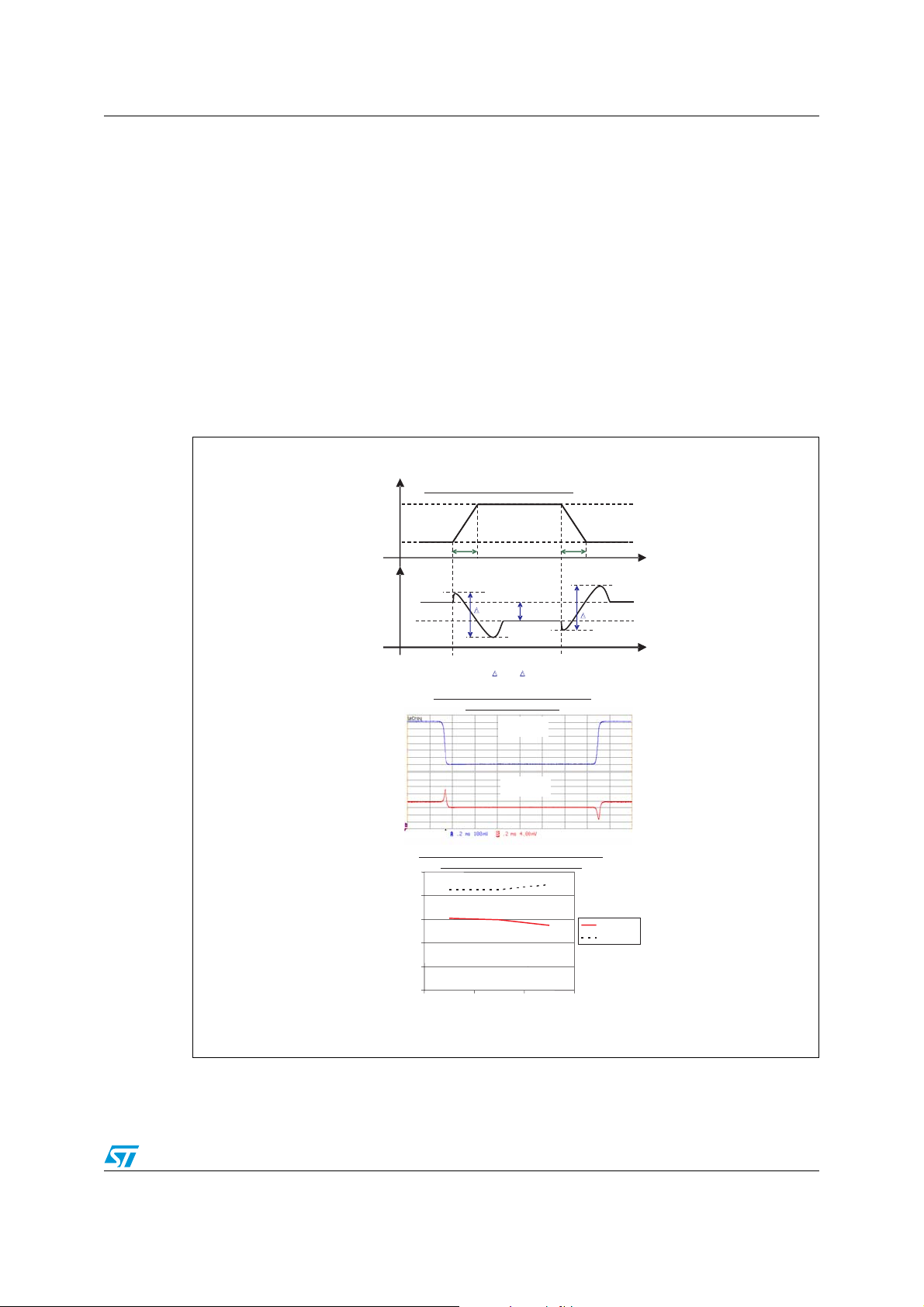
5.1 Line regulation and transient line regulation
The line regulation (LiR) is a static variable that indicates the change in the output voltage of
the voltage controller ΔV
voltage. By contrast the line transient response (LiTr) represents dynamic peak value to be
observed during the change in input voltage
Thermal effects due to changes in the junction temperature are circumvented with pulsed
voltage during the test and are to be taken into account separately.
(at constant load) when there is a change ΔV
out
at the input
bat
The figure shows the boundary conditions for t
rise
, t
fall
, and ΔV
to be taken as the basis of
bat
the measurement of the line transient response without additional decoupling of the supply
voltage by a buffer capacity C
only in the case of decoupling of the supply voltage with such a capacity C
which the values for t
rise
and t
. The values defined in the specification apply, however,
bat
are influenced to some extent.
fall
, as a result of
bat
Figure 13. Line regulation and transient line regulation
Vbat
VbatH
VbatL
Vout
Vbat
Vout
Static and dynamic line regulation
t
= t
rise
tr
Vrise
Line Regulation: LiR=f(VbatH,VbatL)
Line Transient: LiTr = MAX(
Transient line regulation measurement
4V
3.4 V
Vrise, Vfall) –LiR(VbatH,VbatL)
Typcial values at 25° C
X: 0.2 ms/div
Y: 100 mV/div
X: 0.2 ms/div
Y: 4 mV/div
LiR
t
= t
fall
tr
Vfall
Time
Time
Line regulation (LiR) and Line transient (LiTr)
versus temperature (typical values
5
4
3
2
1
0
-10 25 85
LiR (mV)
LiTr (mV)
Temperature (°c)
Doc ID 15194 Rev 2 17/23

Low drop out voltage regulator EMIF06-SD03F3
5.2 Load regulation and transient load regulation
The load regulation (LdR) is a static variable that indicates the change in output voltage of
the voltage controllor ΔV
current ΔI
. By contrast the load transient response (LdTr) represents the dynamic peak
out
value to be observed during load variation.
Thermal effects due to changes in the junction temperature are circumvented by testing with
pulsed load and are to be taken into account separately.
(at constant input voltage) in the event of a change in the load
out
The figure shows the boundary conditions for t
rise
the measurement of the load transient response.
Figure 14.
Load regulation and transient load regulation
Iout
IoutH
IoutL
Vout
Iout
Static and dynamic load regulation
t
= t
fall
tr
Vrise
Load Regulation: LdR=f(IoutH,IoutL)
Load Transient: LdTr = MAX(
Transient load regulation measurement
(typical values at 25° C)
Vrise, Vfall) –LdR(IoutH,IoutL)
LdR
, t
, and ΔI
fall
t
rise
= t
tr
Vfall
X: 50µs/div
Y: 50mA/div
to be taken as the basis for
out
Time
Time
Vccb
Load regulation (LdR) and Load transient (LdTr)
60
50
40
30
20
10
versus temperature (typical values
0
-10 25 85
18/23 Doc ID 15194 Rev 2
X: 50µs/div
Y: 10mV/div
LdR (mV)
LdTr (mV)
Temperature (°c)

EMIF06-SD03F3 Application schematic
5.3 Dropout definition
The dropout voltage (VDO) is measured by decreasing the input voltage till the output
voltage will drop by 100 mV compared to the output voltage measured at the specified
minimum supply voltage (3.1 V).
Worst case for dropout is maximum die temperature and maximum current load. This is
done statically.
Figure 15.
Dropout definition
V(Vbat)
V(Vout)
2.888e+00
VDO
2.772e+00
2.888e+00
-2.122e-01
6 Application schematic
Figure 16. Application schematic
1.8 V
Vbat
3.100e+00
Base
3.100e+00
2.873e+00
100 mV
B3
VccA
GND
Vbat
GND
C4
A4
DAT0 -B
DAT1 -B
DAT3 -B
VccB
CD
WP
CMD-B
CLK-B
B4
D3
E4
26
36
3
12
10
CVccA
Enable
CMD dir
CMD
CLK
CLK feedback
DATA dir
DATA 0 - 3
C2
Enable
A2
D2
C1
C1
A3
E3
D1
E1
A1 12
B1
EMIF06-SD03F3
CMD.dir
CMD.h
CLK.h
CLK.f
DAT0.dir
DAT123.dir
DAT0.h
DAT1.h
DAT2.h DAT2-B
DAT3.h
C3
Cbat
Cout
3.0 V
9
DAT2
1
DAT3/CD/CS
2
CMD
3
VSS1
4
VDD
5
CLK
6
VSS2
7
DAT0
8
DAT1
Doc ID 15194 Rev 2 19/23

Ordering information scheme EMIF06-SD03F3
EMIF
7 Ordering information scheme
Figure 17. Ordering information scheme
yy - xx zz F3
EMI filter
Number of lines
Information
x = resistance value (ohm)
z = capacitance value / 10 (pF)
or
2 letters = application
2 digits = version
Package
F = Flip Chip
3 = Lead-free, pitch = 400 µm
8 Package information
In order to meet environmental requirements, ST offers these devices in different grades of
ECOPACK
specifications, grade definitions and product status are available at: www.st.com
ECOPACK
Figure 18. Flip Chip dimensions
®
packages, depending on their level of environmental compliance. ECOPACK®
®
is an ST trademark.
400 µm ± 40
400 µm ± 40
2.1 mm ± 30 µm
255 µm± 40
2.1 mm ± 30 µm
.
605 µm ± 55
20/23 Doc ID 15194 Rev 2
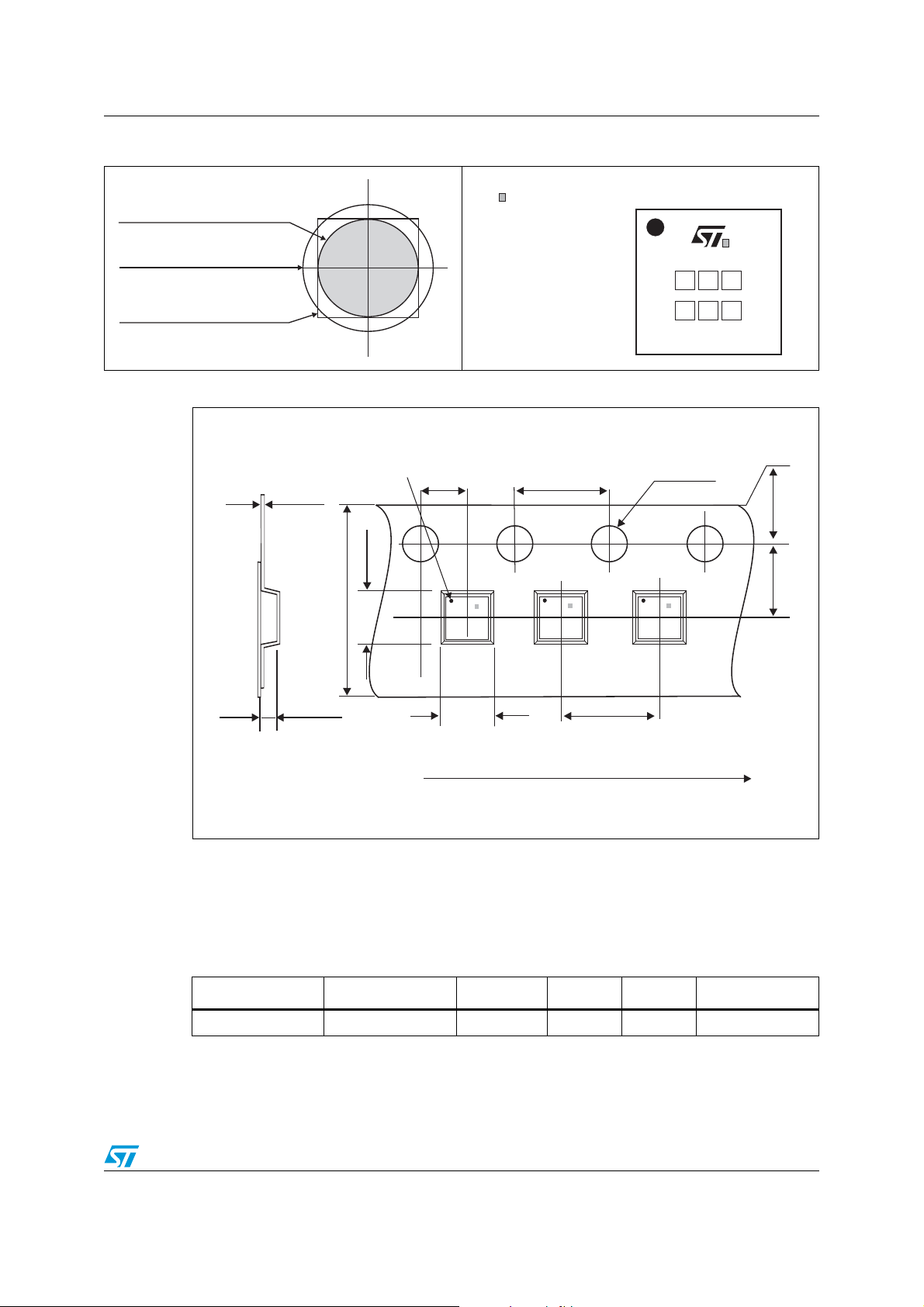
EMIF06-SD03F3 Ordering information
Figure 19. Footprint recommendations Figure 20. Marking
Copper pad Diameter:
220 µm recommended
260 µm maximum
Solder mask opening:
300 µm minimum
Solder stencil opening :
220 µm recommended
Dot, ST logo
ECOPACK status
xx = marking
z = manufacturing location
yww = datecode
(y = year
ww = week)
Figure 21. Flip Chip tape and reel specifications
Dot identifying Pin A1 location
2.0 ± 0.05
0.20 ± 0.02
2.25
4.0 ± 0.1
xyxwz
w
Ø 1.55 ± 0.1
1.75 ± 0.1
8.0 ± 0.3
0.69 ± 0.05
All dimensions in mm
xxz
yww
9 Ordering information
Table 14. Ordering information
Order code Marking Package Weight Base qty Delivery mode
ST
Note: More information is available in the application notes:
EMIF06-SD03F3 HY Flip Chip 5.46 mg 5000 Tape and reel (7”)
AN2348 :"Flip Chip : Package description and recommendations for use"
AN1751 : EMI Filters: Recommendations and measurements
ST
xxz
yww
2.25
4.0 ± 0.1
User direction of unreeling
ST
xxz
yww
3.5 ± 0.1
Doc ID 15194 Rev 2 21/23

Revision history EMIF06-SD03F3
10 Revision history
Table 15. Document revision history
Date Revision Changes
21-Nov-2008 1 First issue
11-Feb-2010 2 AC timing characteristics updated in Ta b l e 1 1 .
22/23 Doc ID 15194 Rev 2

EMIF06-SD03F3
Please Read Carefully:
Information in this document is provided solely in connection with ST products. STMicroelectronics NV and its subsidiaries (“ST”) reserve the
right to make changes, corrections, modifications or improvements, to this document, and the products and services described herein at any
time, without notice.
All ST products are sold pursuant to ST’s terms and conditions of sale.
Purchasers are solely responsible for the choice, selection and use of the ST products and services described herein, and ST assumes no
liability whatsoever relating to the choice, selection or use of the ST products and services described herein.
No license, express or implied, by estoppel or otherwise, to any intellectual property rights is granted under this document. If any part of this
document refers to any third party products or services it shall not be deemed a license grant by ST for the use of such third party products
or services, or any intellectual property contained therein or considered as a warranty covering the use in any manner whatsoever of such
third party products or services or any intellectual property contained therein.
UNLESS OTHERWISE SET FORTH IN ST’S TERMS AND CONDITIONS OF SALE ST DISCLAIMS ANY EXPRESS OR IMPLIED
WARRANTY WITH RESPECT TO THE USE AND/OR SALE OF ST PRODUCTS INCLUDING WITHOUT LIMITATION IMPLIED
WARRANTIES OF MERCHANTABILITY, FITNESS FOR A PARTICULAR PURPOSE (AND THEIR EQUIVALENTS UNDER THE LAWS
OF ANY JURISDICTION), OR INFRINGEMENT OF ANY PATENT, COPYRIGHT OR OTHER INTELLECTUAL PROPERTY RIGHT.
UNLESS EXPRESSLY APPROVED IN WRITING BY AN AUTHORIZED ST REPRESENTATIVE, ST PRODUCTS ARE NOT
RECOMMENDED, AUTHORIZED OR WARRANTED FOR USE IN MILITARY, AIR CRAFT, SPACE, LIFE SAVING, OR LIFE SUSTAINING
APPLICATIONS, NOR IN PRODUCTS OR SYSTEMS WHERE FAILURE OR MALFUNCTION MAY RESULT IN PERSONAL INJURY,
DEATH, OR SEVERE PROPERTY OR ENVIRONMENTAL DAMAGE. ST PRODUCTS WHICH ARE NOT SPECIFIED AS "AUTOMOTIVE
GRADE" MAY ONLY BE USED IN AUTOMOTIVE APPLICATIONS AT USER’S OWN RISK.
Resale of ST products with provisions different from the statements and/or technical features set forth in this document shall immediately void
any warranty granted by ST for the ST product or service described herein and shall not create or extend in any manner whatsoever, any
liability of ST.
ST and the ST logo are trademarks or registered trademarks of ST in various countries.
Information in this document supersedes and replaces all information previously supplied.
The ST logo is a registered trademark of STMicroelectronics. All other names are the property of their respective owners.
© 2010 STMicroelectronics - All rights reserved
Australia - Belgium - Brazil - Canada - China - Czech Republic - Finland - France - Germany - Hong Kong - India - Israel - Italy - Japan -
STMicroelectronics group of companies
Malaysia - Malta - Morocco - Philippines - Singapore - Spain - Sweden - Switzerland - United Kingdom - United States of America
www.st.com
Doc ID 15194 Rev 2 23/23
 Loading...