

6-line EMI filter and ESD protection for audio interface
Features
■ 4-line EMI filter and ESD protection for internal
and external (headset) microphone
■ 2-line EMI filter and ESD protection for headset
speaker
Benefits
■ EMI (I/O) low-pass filter
■ High efficiency EMI filter
■ Very low PCB space consumption: 4.6 mm
■
Very thin package: 0.65 mm
■ High efficiency in ESD suppression
■ High reliability offered by monolithic integration
■ High reduction of parasitic elements through
integration and wafer level packaging
Complies with following standards
■ IEC 61000-4-2 level 4 external pins
– 15 kV (air discharge)
– 8 kV (contact discharge)
■ IEC 61000-4-2 level 1 internal pins
– 2 kV (air discharge)
– 2 kV (contact discharge)
Applications
ESD protection and EMI/RFI filtering for the audio
bottom connector interface, where EMI filtering in
ESD sensitive equipment is required:
■ Mobile phones and communication systems
■ Wireless modules
2
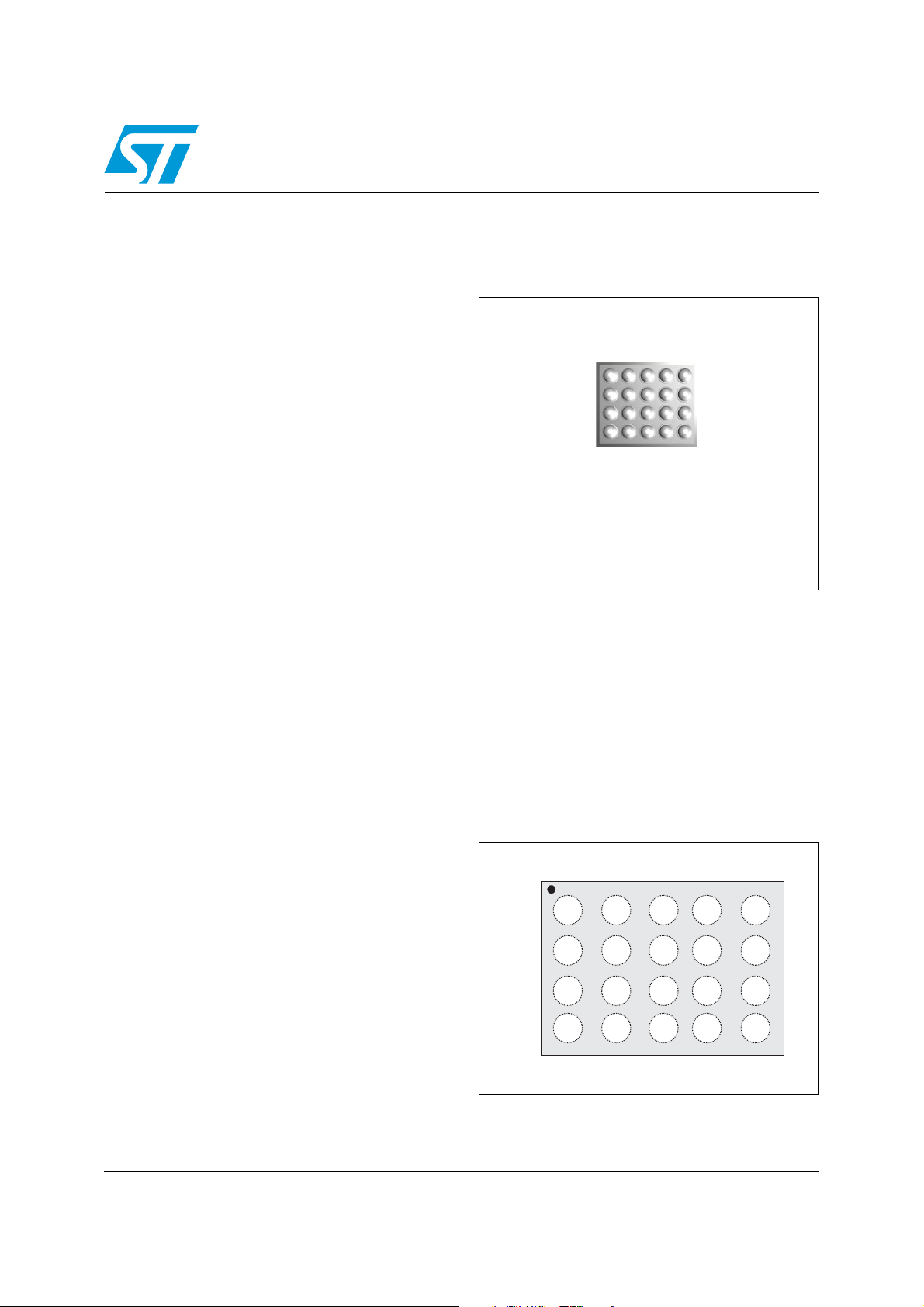
EMIF06-AUD01F2
Flip chip package, 20 bumps
Description
The EMIF06-AUD01F2 is a highly integrated
device designed to suppress EMI/RFI noise in all
systems subjected to electromagnetic
interference. The flip chip packaging means the
package size is equal to the die size.
This filter includes ESD protection circuitry, which
prevents damage to the application when it is
subjected to ESD surges up to 15 kV.
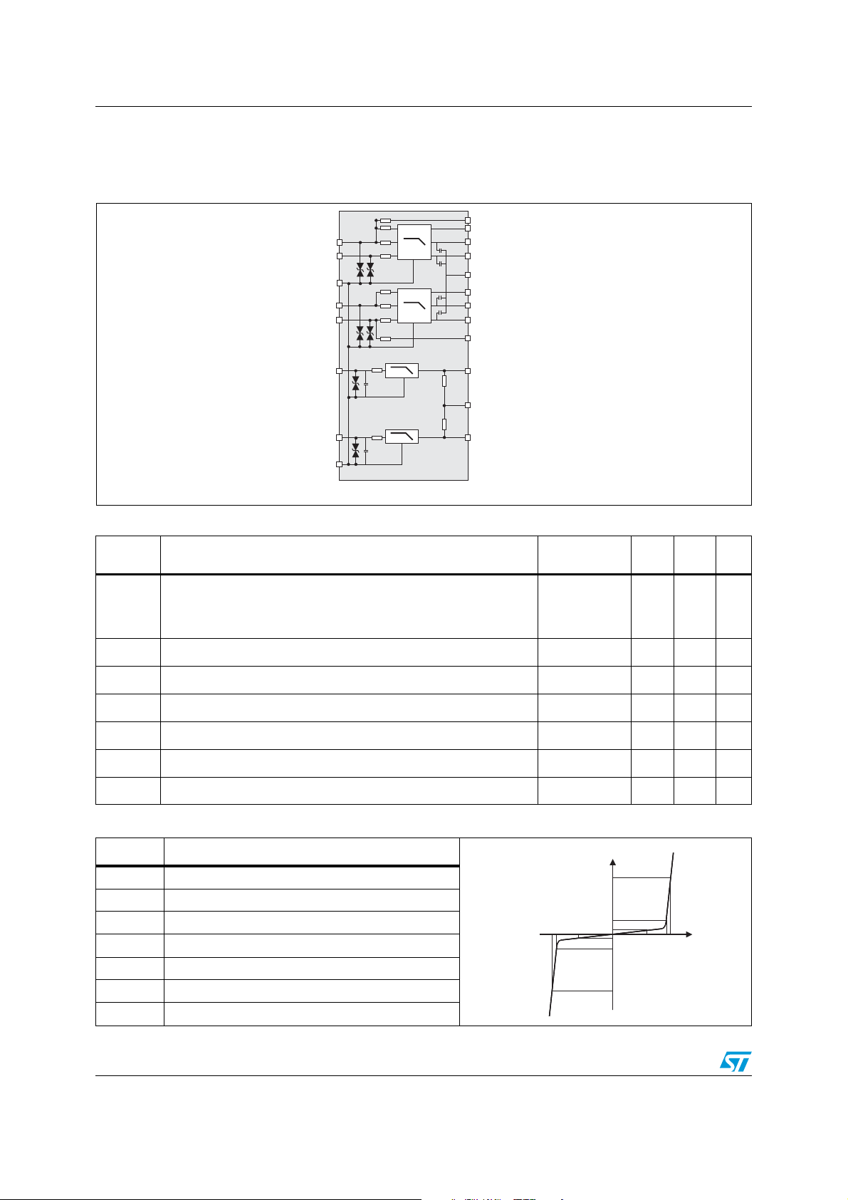
Figure 1. Pin configuration
12345
GND
Int
MIC2N
int
SPK_R SPK_L
HOOK
BIAS2
GND
SPK_L
int
MIC1P MIC2N MIC2P
A
MIC1N
B
C
GND
BIAS1
MIC1P
int
MIC1N
D
BIAS3
int
MIC2P
int
SPK_R
int
PHG
Silicon side
February 2008 Rev 1 1/14
www.st.com
Characteristics EMIF06-AUD01F2
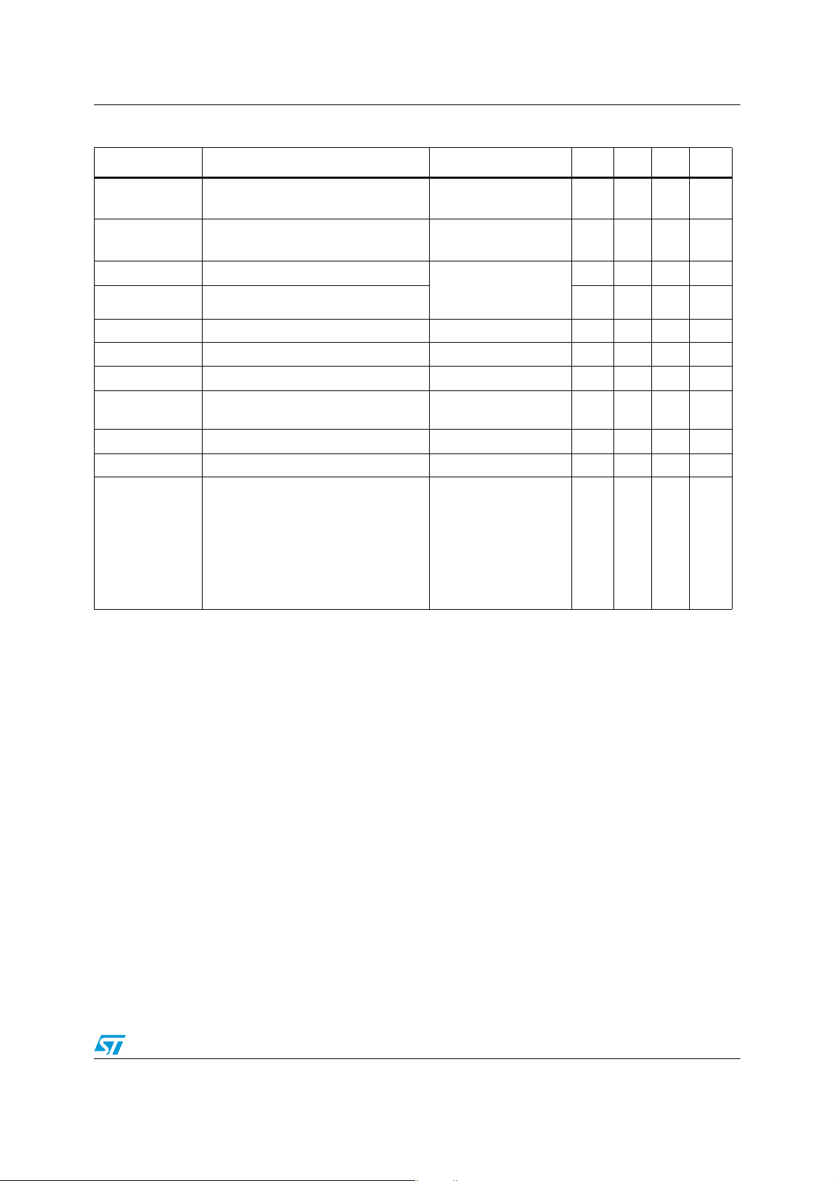
1 Characteristics
Figure 2. Circuit schematic
MIC2_P-ext
MIC2_N-ext
GND-ext
MIC1_P-ext
MIC1_N-ext
R1
R2
R3
R4
R6
R7
R8
R9
C1
C2
C3
C4
HOOK
BIAS2
MIC2_P-int
MIC2_N-int
GND-int
BIAS1
MIC1_P-int
MIC1_N-int
BIAS3
SPK_R-ext
SPK_L-ext
GND-ext
R10
C5
R11
C6
C1 to C4 = 1.3 nF typical
Table 1. Absolute ratings (limiting values)
Symbol Parameter
IEC61000-4-2 air discharge on external lines
V
IEC61000-4-2 contact discharge on external lines
pp
IEC61000-4-2 air discharge on internal lines
IEC61000-4-2 contact discharge on internal lines
P
I
P
SPK
T
T
SPK
total
op
stg
Continuous power dissipation per channel SPK_L, SPK_R T
Continuous current per channel SPK_L, SPK_R T
Total continuous power dissipation T
Operating temperature range -40 +85 °C
Storage temperature range -40 +125 °C
R12
R13
SPK_R-int
PHG (Phantom Ground)
SPK_L-int
Test
conditions
Min Max Unit
15
15
kV
2
2
= 85 °C 180 mW
amb
= 85 °C 135 mA
amb
= 85 °C 285 mW
amb
T
Junction temperature +125 °C
j
Table 2. Electrical characteristics - definitions (T
Symbol Parameters
V
I
RM
V
V
R
I
C
Breakdown voltage
BR
Leakage current @ V
Stand-off voltage
RM
Clamping voltage
CL
Dynamic impedance
d
Peak pulse current
PP
Input capacitance per line
line
RM
2/14
amb
= 25 °C)
VCL
I
I
PP
IR
IRM
VRMVBR
IRM
IR
IPP
V
VCL
VBRVRM
EMIF06-AUD01F2 Characteristics
Table 3. Electrical characteristics - values (T
= -40 °C to + 85 °C unless otherwise specified)
amb
Symbol Parameter Test conditions Min Typ Max Unit
V
BR
I
RM
(1)
C1-C4
(1)
C5-C6
(2)
R1
(2)
R2
R3,R4, R7, R8
(2)
R6, R9
R10, R11
R12, R13
(3)
(2)
Diode reverse breakdown voltage
Leakage current through clamping
diodes
Capacitance on MIC lines V = 0 V, F = 1 MHz,
Channel Capacitance SPK_L, SPK_R 60 pF
Hook Pull up resistance 47 kΩ
External Microphone Pull up resistance 2.2 kΩ
(2)
Microphone Serial Resistance 100 Ω
Internal Microphone Pull up and
Pull down resistance
SPK Serial Resistance 10 Ω
SPK PHG Resistance 15 kΩ
IR = 1 mA
T
= 25 °C
amb
= 3 V DC per line
V
R
T
= 25 °C
amb
V
= 30 mV
OSC
= 25 °C
T
amb
= 0 - 2.4 V,
V
dc
14.0 V
1.3 nF
1kΩ
(4)
F = 20 Hz - 20 kHz,
R
= 600 Ω,
MICx channel
THD
Distortion
V
R
T
gen
out
load
amb
= 1.5 V
= 200 kΩ,
= 25 °C
PP
Balanced
(or differential mode)
1. Capacitor tolerance ±30%
2. Resistor tolerances ±10%
3. Resistor tolerances ±20%
4. See Figure 20 and Figure 21
0.5 µA
-75 dB(A)
3/14
Characteristics EMIF06-AUD01F2
1.1 RF filtering
The low signal level on the analog inputs and the pulsed transmitter in the phone are a
combination that requires efficient RF-filtering. RF-rectification must be avoided.
Therefore, the stop band attenuation is optimized for the frequency bands 800-2480 MHz.
Table 4. Stop band performance 800 - 2480 MHz
Attenuation
Channel Test conditions
Min Typ Max Unit
MIC1_x to MIC1_x-int R
MIC2_x to MIC2_x-int R
MIC1_P to BIAS1 R
MIC2_P to BIAS2 R
SPK_x to SPK_x-int R
Table 5. Stop band performance 10 - 800 MHz
source
source
source
source
source
= 50 Ω, R
= 50 Ω, R
= 50 Ω, R
= 50 Ω, R
= 50 Ω, R
Channel Test conditions
MIC1_x to MIC1_x-int R
MIC2_x to MIC2_x-int R
MIC1_P to BIAS1 R
MIC2_P to BIAS2 R
source
source
source
source
= 50 Ω, R
= 50 Ω, R
= 50 Ω, R
= 50 Ω, R
1.2 Attenuation characteristics
Figure 3. S21 attenuation measurement
MIC1_P and MIC1_N lines
(50 Ω / 50 Ω)
0.00
dB
-10.00
= 1 kΩ 25 dB
load
= 1 kΩ 25 dB
load
= 1 kΩ 25 dB
load
= 1 kΩ 25 dB
load
= 1 kΩ 25 dB
load
Attenuation
Min Typ Max Unit
= 1 kΩ 20 dB
load
= 1 kΩ 20 dB
load
= 1 kΩ 20 dB
load
= 1 kΩ 20 dB
load
Figure 4. S21 attenuation measurement
MIC1_P and MIC1_N lines
(50 Ω / 1 KΩ simulation)
0
dB
-10
-20.00
-30.00
-40.00
-50.00
MIC1_N line
F/Hz
R = 50 / R = 50
source load
ΩΩ
-60.00
100.0k 1.0M 10.0M 100.0M 1.0G
MIC1_P line
4/14
-20
-30
-40
-50
-60
100k 1M 10M 100M 1G
MIC1_P line MIC1_N line
F/Hz
R = 50 / R = 1 K
source load
ΩΩ
EMIF06-AUD01F2 Characteristics
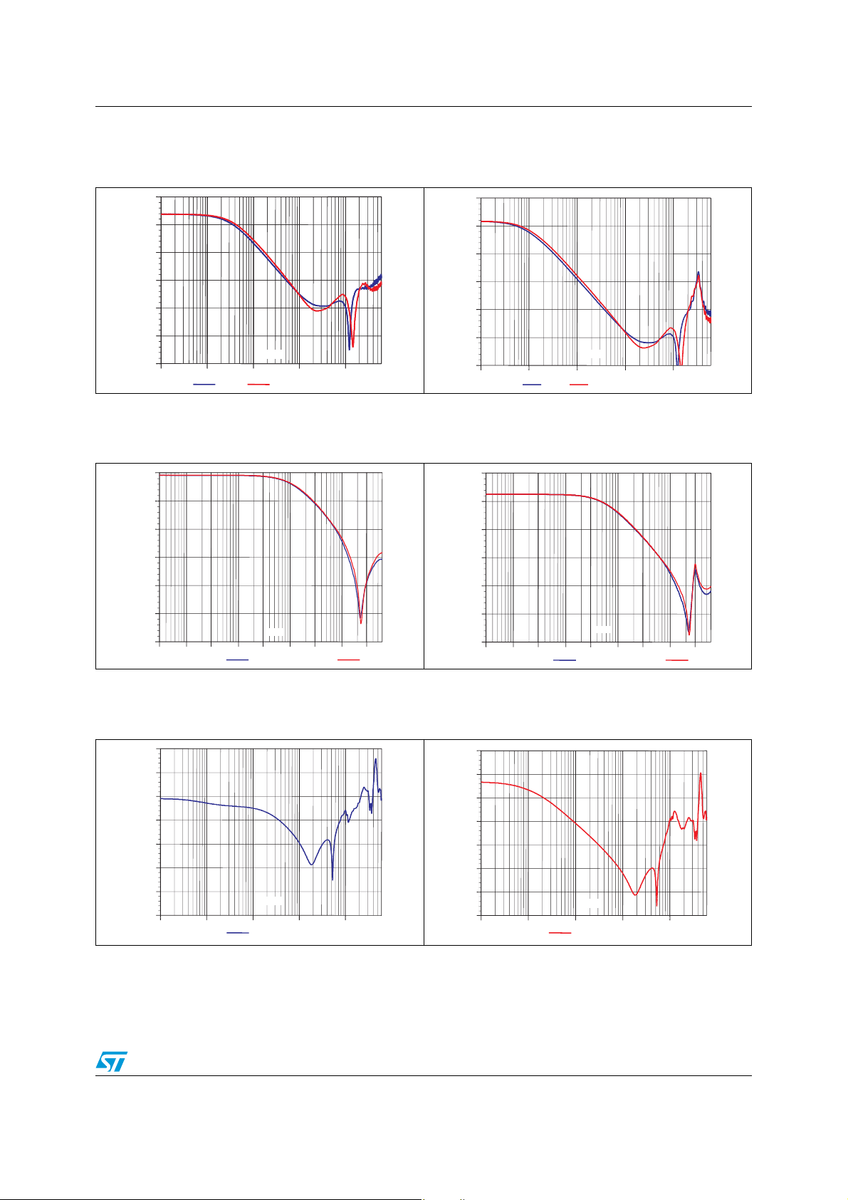
Figure 5. S21 attenuation measurement
MIC2_P and MIC2_N lines
(50 Ω / 50 Ω)
0.00
dB
-10.00
-20.00
-30.00
-40.00
-50.00
-60.00
100.0k 1.0M 10.0M 100.0M 1.0G
MIC2_P line
MIC2_N line
F/Hz
R = 50 / R = 50
source load
ΩΩ
Figure 7. S21 attenuation measurement
SPK_L and SPK_R lines
(50 Ω / 50 Ω)
0.00
dB
- 10.00
- 20.00
Figure 6. S21 attenuation measurement
MIC2_P and MIC2_N lines
(50 Ω / 1 KΩ simulation)
0
dB
-10
-20
-30
-40
-50
-60
100k 1M 10M 100M 1G
MIC2_P line MIC2_N line
F/Hz
R = 50 / R = 1 K
ΩΩ
source load
Figure 8. S21 attenuation measurement
SPK_L and SPK_R lines
(50 Ω / 1 KΩ simulation)
0.00
dB
- 10.00
- 20.00
- 30.00
- 40.00
- 50.00
- 60.00
300.0k 1.0M 3.0M 10.0M 30.0M 100.0M 300.0M 1.0G 3.0G
SPK_R line
f/Hz
F/Hz
SPK_L line
Figure 9. S21 attenuation measurement
MIC1_P and BIAS1 lines
(50 Ω / 50 Ω)
0.00
dB
- 10.00
- 20.00
- 30.00
- 40.00
- 50.00
- 60.00
- 70.00
100.0k 1.0M 10.0M 100.0M 1.0G
Mic1P/BIAS1 50
F/Hz
R = 50 / R = 50
source load
ΩΩ
- 30.00
- 40.00
- 50.00
F/Hz
- 60.00
300.0k 1.0M 3.0M 10.0M 30.0M 100.0M 300.0M 1.0G 3.0G
SPK_R line Sim
f/Hz
SPK_L line Sim
Figure 10. S21 attenuation measurement
MIC1_P and BIAS1 lines
(50 Ω / 1 KΩ simulation)
0.00
dB
- 10.00
- 20.00
- 30.00
- 40.00
- 50.00
- 60.00
- 70.00
100.0k 1.0M 10.0M 100.0M 1.0G
Mic1P/BIAS1 1k
F/Hz
R = 50 / R = 1 k
source load
ΩΩ
5/14
 Loading...