

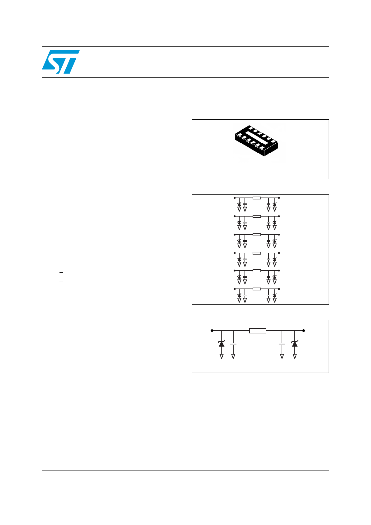
Features
EMIF06-1005N12
6-line IPAD™, low capacitance
EMI filter and ESD protection in narrow micro QFN package
■ EMI symmetrical (I/O) low-pass filter
■ High efficiency in EMI filtering at frequencies
from 900 MHz to 1.8 GHz
■ Very low PCB space consumption:
2.5 mm x 1.2 mm
■ Very thin package: 0.55 mm max
■ High efficiency in ESD suppression on inputs
pins (IEC 61000-4-2 level 4)
■ High reliability offered by monolithic integration
■ High reduction of parasitic elements through
integration and wafer level packaging
■ Lead-free package
Complies with the following standards
■ IEC 61000-4-2 level 4 input and output pins
–
+ 15 kV (air discharge)
–
+ 8 kV (contact discharge)
■ MIL STD 883G - Method 3015-7 Class 3B
(all pins)
Applications
Where EMI filtering in ESD sensitive equipment is
required:
■ LCD and camera for mobile phones
■ Computers and printers
■ Communication systems
■ MCU boards
■ Keypad for portable equipment
12
1
µQFN-12L
Figure 1. Pin configuration (top view)
1 Input Output 12
2 Input
3 Input
4 Input
5 Input
6 Input
Output 11
Output 10
Output 9
Output 8
Output 7
Figure 2. Basic cell configuration
Input
Typical line capacitance = 45 pF @ 0 V
100 Ω
Description
Output
EMIF06-1005N12 is a 6-line, highly integrated
device designed to suppress EMI/RFI noise in all
systems exposed to electromagnetic
interference.This filter includes ESD protection
circuitry, which prevents damage to the
TM: IPAD is a trademark of STMicroelectronics.
July 2011 Doc ID 16959 Rev 2 1/12
application when subjected to ESD surges up to
15 kV on the input pins.
www.st.com
12
Characteristics EMIF06-1005N12
1 Characteristics
Table 1. Absolute ratings (limiting values)
Symbol Parameter and test conditions Value Unit
ESD discharge IEC 61000-4-2, level 4
air discharge
contact discharge
V
ESD-Machine Model :
PP
(MM: C = 200 pF, R = 25 Ω L = 500 nH)
ESD-Charged Device Model:
(JESD22-C101D)
Junction temperature at T
T
j
T
T
Operating temperature range - 40 to + 85 °C
op
Storage temperature range - 55 to + 150 °C
stg
= 25 °C 125 °C
amb
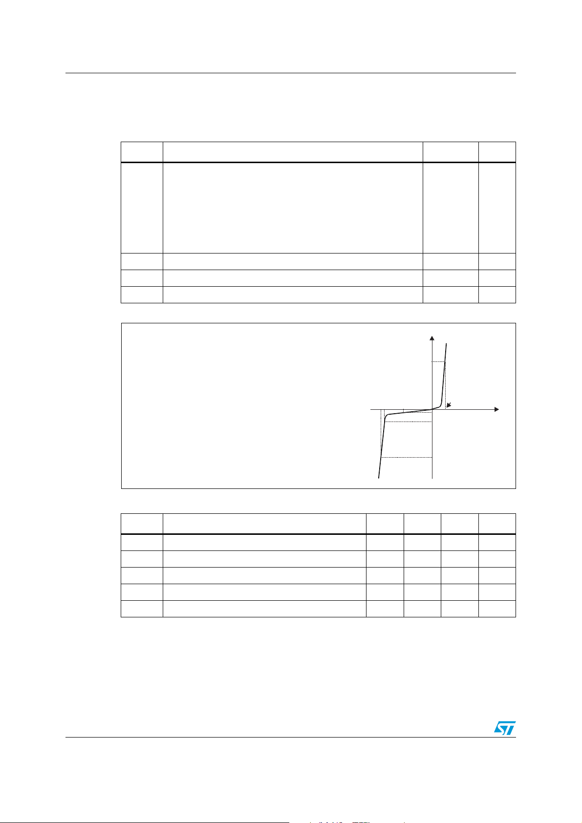
Figure 3. Electrical characteristics (definitions)
15
15
2
kV
1
Symbol Parameter
V = Breakdown voltage
BR
V = Clamping voltage
CL
I = Leakage current @ V
RM RM
V = Stand-off voltage
RM
I = Forward current
F
I = Peak pulse current
PP
I = Breakdown current
R
V = Forward voltage drop
F
R
I = Forward current
PP
R = Series resistanc between input and output
C = Input capacitance per line
Table 2. Electrical characteristics (T
= Dynamic impedance
d
I/O
line
amb
= 25 °C)
V
V
CL
BR
I
I
F
V
V
RM
F
I
RM
I
R
I
PP
Symbol Test conditions Min. Typ. Max. Unit
V
BRIR
V
F
I
RM
R
I/O
C
line
= 1 mA 6 8 10 V
IF = 10 mA 0.5 1 1.5 V
VRM = 3 V per line 200 nA
Tolerance ± 15% 85 100 115 Ω
V
= 0 V, V
line
= 30 mV, F = 1 MHz 38 45 52 pF
osc
V
2/12 Doc ID 16959 Rev 2
EMIF06-1005N12 Characteristics
Figure 4. S21 attenuation measurement Figure 5. Analog cross talk measurements
S21 (dB)
0.0
- 10
- 20
I2-O2
I2-O2
I4-O4
I4-O4
- 30
I1-O1
I1-O1
I3-O3
I3-O3
I5-O5
I5-O5
I6-O6
I6-O6
- 40
- 50
F = 110 MHz
C
S21(dB)
F = 900 MHz
-35
- 60
300k 1M 3M 10M 30M 100M 300M 1G 3G
S21(dB)
F = 1.8 GHz
-31
V = 0V
BIAS
Figure 6. ESD response to IEC 61000-4-2
(+8 kV contact discharge).
Remaining voltage on filter output
C1
5 V/Div
OUTPUT
V max
CL
27.2 V
VCL@
t = 30 ns
4.6 V
VCL@
t = 100 ns
3.3 V
F(Hz)
XTalk (dB)
0.0
- 10
- 20
- 30
- 40
I2-O5
I2-O3
- 50
- 60
- 70
- 80
- 90
- 100
- 110
- 120
- 130
300k 1M 3M 10M 30M 100M 300M 1G 3G
V = 0V
BIAS
F(Hz)
Figure 7. ESD response to IEC 61000-4-2
(-8 kV contact discharge).
Remaining voltage on filter output
5 V/Div
C1
OUTPUT
V max
CL
-20.7 V
VCL@
t = 30 ns
-3.2 V
VCL@
t = 100 ns
-787 mV
20 ns/Div
Figure 8. ESD test conditions for figure 6 and figure 7
D.U.T
Attenuator 20…60dB
50 Ohm
20 ns/Div
>500MHz Oscilloscope with
50 Ohm input mode
Doc ID 16959 Rev 2 3/12
Characteristics EMIF06-1005N12
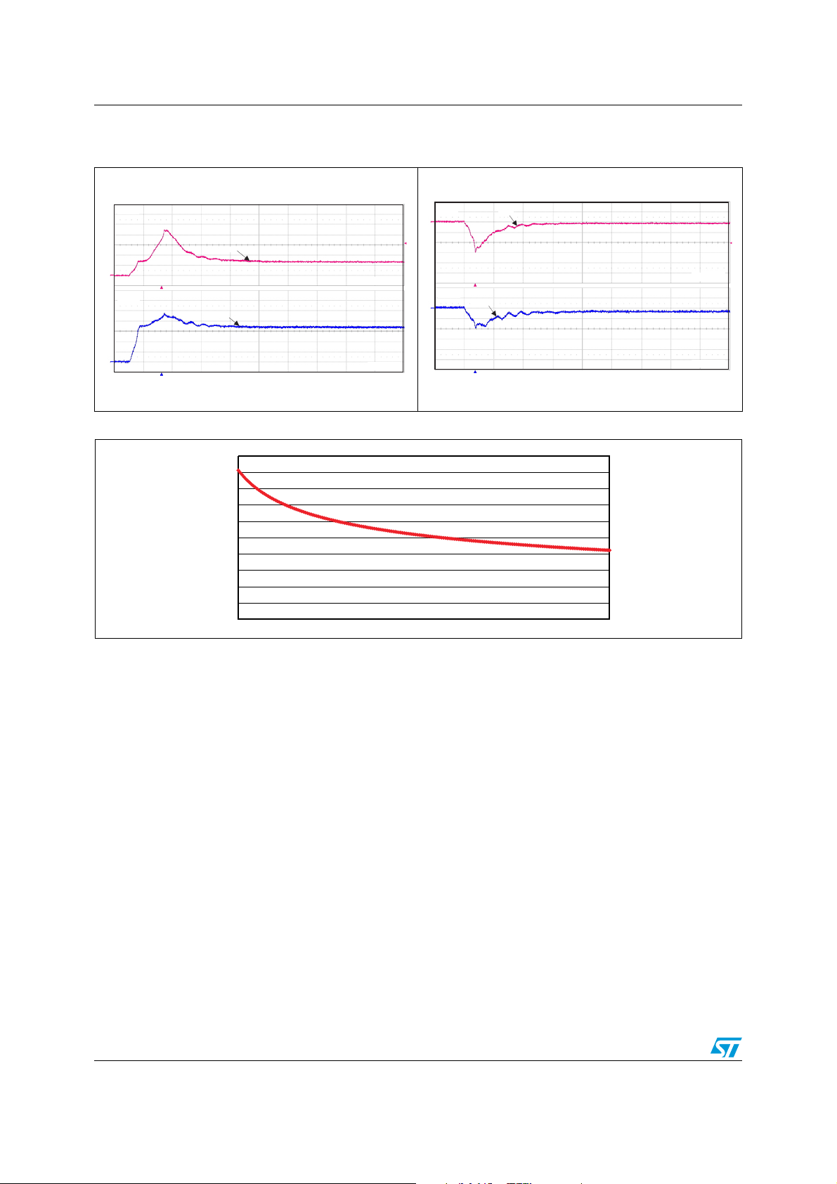
Figure 9. ESD response to IEC 61000-4-2
(+15 kV air discharge) on one line
Figure 10. ESD response to IEC 61000-4-2
(-15 kV air discharge) on one line
5 V/Div
INPUT
C2
2 V/Div
OUTPUT
C3
100 ns/Div
100 ns/Div
C2
C3
Figure 11. Line capacitance versus applied voltage
C(pF)
50
45
40
35
30
25
20
15
10
5
0
0123456
5 V/Div
2 V/Div
OUTPUT
INPUT
V (V)
R
100 ns/Div
100 ns/Div
4/12 Doc ID 16959 Rev 2
 Loading...