

®
4 LINES LOW CAPACITANCE EMI FILTER
IPAD™
MAIN APPLICATION
Where EMI filtering in ESD sensitive equipment is
required:
■ LCD and camera for mobile phones
■ Computers and printers
■ Communication systems
■ MCU board
EMIF04-VID01F2
AND ESD PROTECTION
®
DESCRIPTION
The EMIF04-VID01F2 is a 4 lines highly integrated
array designed to suppress EMI / RFI noise in all
systems subjected to electromagnetic interferences.
The EMIF04-VID01F2 Flip-Chip packaging means
the package size is equal to the die size.
Additionally, this filter includes an ESD protection
circuitry which prevents the protected device from
destruction when subjected to ESD surges up to
15 kV.
BENEFITS
■ High efficiency EMI filtering (-40db @ 900MHz)
■ Low line capacitance suitable for high speed
data bus
■ Low serial resistance for camera impedance
adaptation
■ Lead free package
■ Optimized PCB space consuming:
1.92mm x 1.29mm
■ Very thin package: 0.65 mm
■ High efficiency in ESD suppression on inputs
pins (IEC61000-4-2 level 4)
■ High reliability offered by monolithic integration
■ High reducing of parasitic elements through
integration & wafer level packaging
■ Reduce compnents counts and BOM
COMPLIES WITH THE FOLLOWING STANDARDS:
IEC61000-4-2
Level 4 on input pins 15kV (air discharge)
8kV (contact discharge)
MIL STD 883E - Method 3015-6 Class 3
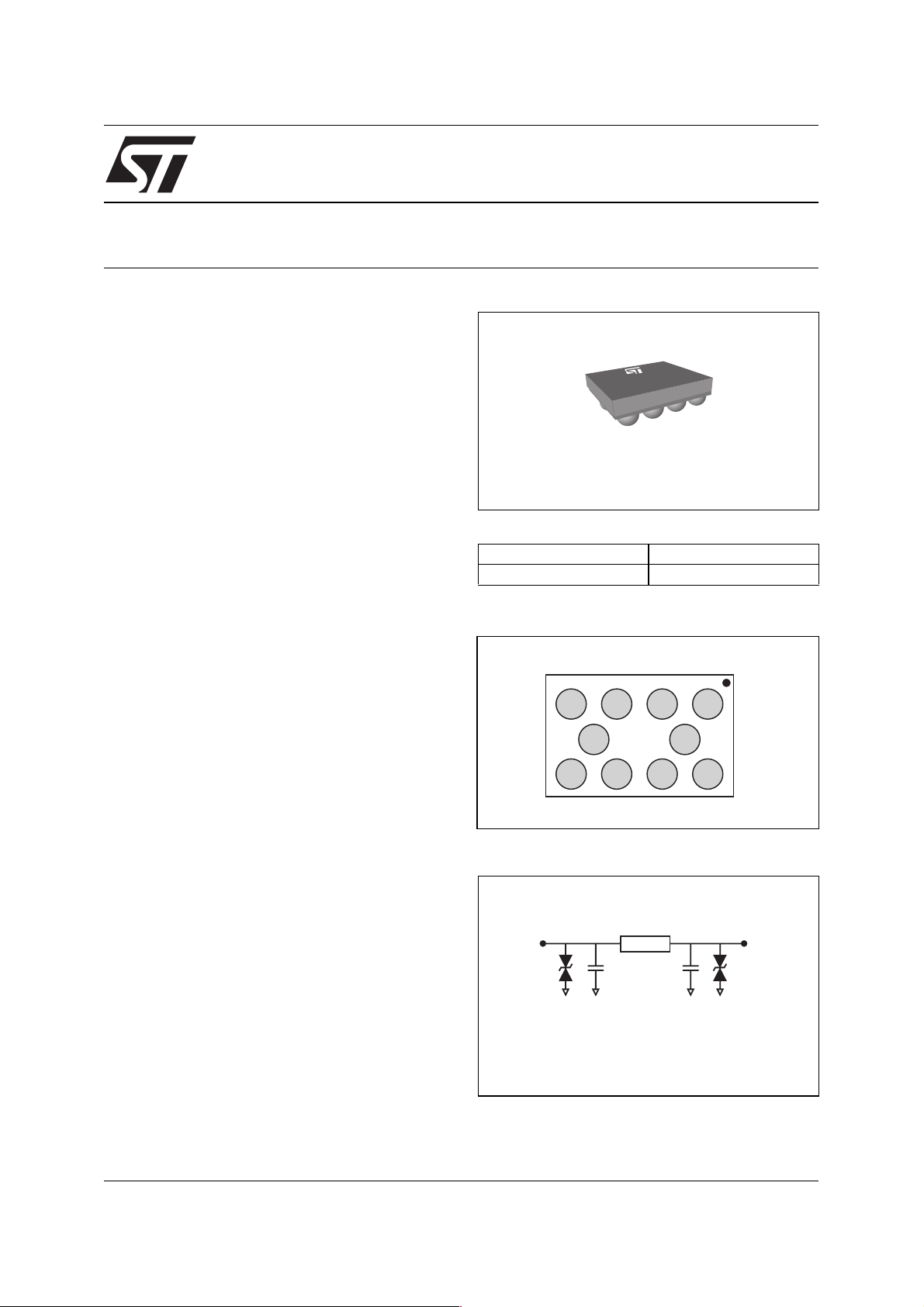
Flip-Chip
(10 Bumps)
Table 1: Order Code
Part Number Marking
EMIF04-VID01F2 GU
Figure 1: Pin Configuration (ball side)
654 321
I3
I4
Gnd Gnd
O4
O3
I2
O2
I1
O1
Figure 2: Configuration
R
Input
R = 100
C = 16pF typ. @ 3V
Ω
LINE
A
B
C
Output
TM: IPAD is a trademark of STMicroelectronics.
REV. 1February 2005
1/6
EMIF04-VID01F2
Table 2: Absolute Ratings (limiting values)
Symbol Parameter and test conditions Value Unit
T
T
op
T
stg
Maximum junction temperature 125 °C
j
Operating temperature range - 40 to + 85 °C
Storage temperature range - 55 to + 150 °C
Table 3: Electrical Characteristics (T
Symbol Parameter
V
I
RM
V
Breakdown voltage
BR
Leakage current @ V
Stand-off voltage
RM
RM
R Series resistance between Input &
Output
C
Input capacitance per line
line
amb
= 25°C)
I
IR
IRM
VRMVBR
IRM
IR
V
V
BRVRM
Symbol Test conditions Min. Typ. Max. Unit
V
I
BR
RM
IR = 1mA
VRM = 3V per line
6810V
500 nA
R I = 10mA 80 100 120 Ω
C
line
VR = 3V DC 1MHz V
OSC
= 30mV
16 19 pF
2/6

EMIF04-VID01F2
Figure 3: S21 (dB) attenuation measurement Figure 4: Analog crosstalk measurement
0
dB
-10
-20
-30
-40
-50
-60
100k 1M 10M 100M 1G
f/Hz
0
dB
-10
-20
-30
-40
-50
-60
-70
-80
-90
-100
100k 1M 10M 100M 1G
f/Hz
Figure 5: ESD response to IEC61000-4-2
(+15kV air discharge) on one input V(in) and on
one output (Vout)
Input
10V/d
Output
10V/d
200ns/d
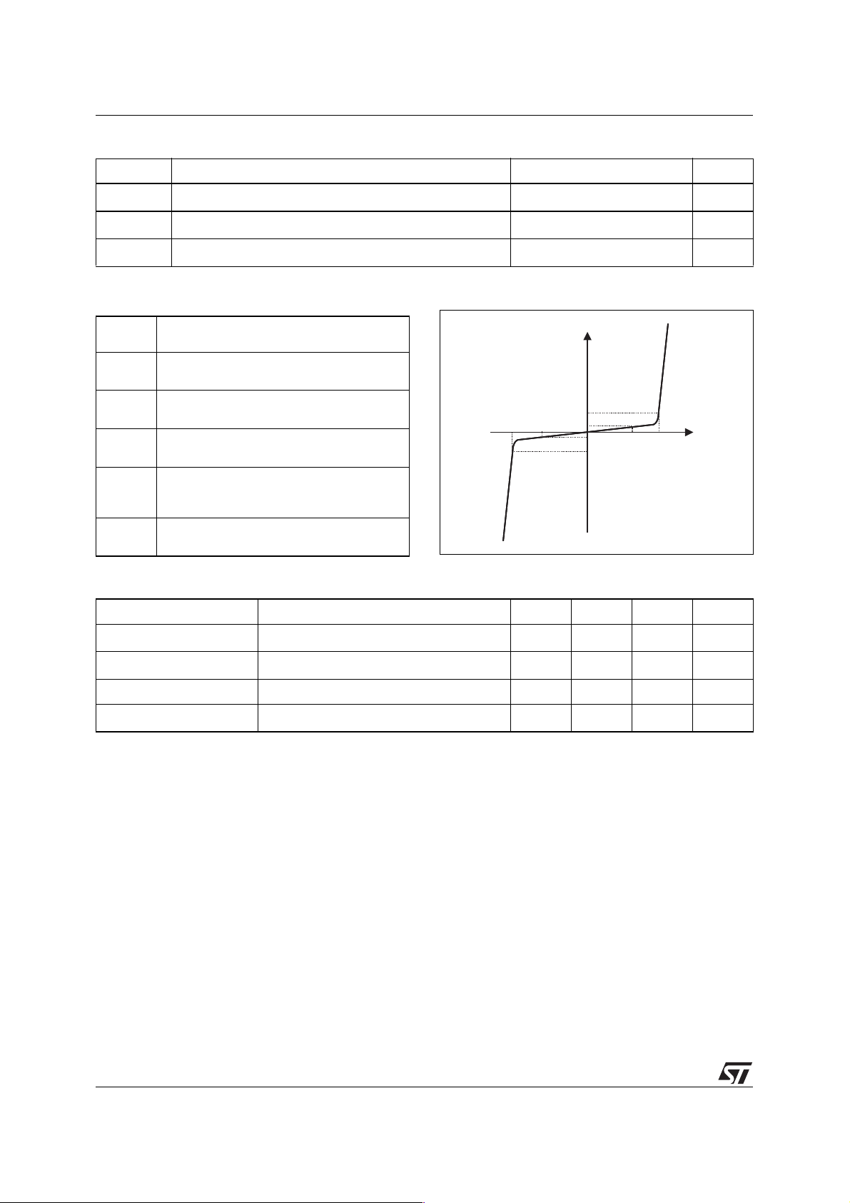
Figure 7: Junction capacitance versus reverse
voltage applied (typical values)
C (pF)
LINE
28
28
26
26
24
24
22
22
20
20
18
18
16
16
14
14
12
12
10
10
0.0 0.5 1.0 1.5 2.0 2.5 3.0
0.0 0.5 1.0 1.5 2.0 2.5 3.0
V (V)
LINE
Figure 6: ESD response to IEC61000-4-2 (-15kV
air discharge) on one input V(in) and on one
output (Vout)
Input
10V/d
Output
10V/d
200ns/d
3/6

EMIF04-VID01F2
5
Figure 8: Ordering Information Scheme
EMI Filter
Number of lines
Information
x = resistance value (Ohms)
z = capacitance value / 10(pF)
or
3 letters = application
2 digits = version
Package
F2 = Leadfree Flip-Chip
x = 1: 500µm, Bump = 315µm
= 2: Leadfree Pitch = 500µm, Bump = 315µm
Figure 9: FLIP-CHIP Package Mechanical Data
EMIF yy - xxx zz Fx
315µm ± 50
500µm ± 50
250µm ± 50
01µm ± 50
1.92mm ± 50µm
435µm ± 50
1.29mm ± 50µm
Figure 10: Foot Print Recommendations Figure 11: Marking
Dot, ST logo
xx = marking
Copper pad Diameter :
250µm recommended , 300µm max
Solder stencil opening : 330µm
Solder mask opening recommendation :
340µm min for 300µm copper pad diameter
z = packaging location
yww = date code
(y = year
ww = week)
365
650µm ± 65
365
220
x
y
240
wxw
E
z
40
All dimensions in µm
4/6

Figure 12: FLIP-CHIP Tape and Reel Specification
EMIF04-VID01F2
Dot identifying Pin A1 location
8 +/- 0.3
0.73 +/- 0.05
All dimensions in mm
yww
xxx
4 +/- 0.1
ST
E
yww
xxx
User direction of unreeling
ST
E
4 +/- 0.1
Ø 1.5 +/- 0.1
yww
xxx
1.75 +/- 0.1 3.5 +/- 0.1
ST
E
Table 4: Ordering Information
Ordering code Marking Package Weight Base qty Delivery mode
EMIF04-VID01F2 GU Flip-Chip 3.6 mg 5000 Tape & reel 7”
Note: More packing informations are available in the application note
AN1235: “Flip-Chip: Package description and recommendations for use”
AN1751: “EMI Filters: Recommendations and measurements”
Table 5: Revision History
Date Revision Description of Changes
15-Feb-2005 1 First issue.
5/6

EMIF04-VID01F2
Information furnished is believed to be accurate and reliable. However, STMicroelectronics assumes no responsibility for the consequences
of use of such information nor for any infringement of patents or other rights of third parties which may result from its use. No license is granted
by implication or otherwise under any patent or patent rights of STMicroelectronics. Specifications mentioned in this publication are subject
to change without notice. This publication supersedes and replaces all information previously supplied. STMicroelectronics products are not
authorized for use as critical components in life support devices or systems without express written approval of STMicroelectronics.
The ST logo is a registered trademark of STMicroelectronics.
All other names are the property of their respective owners
© 2005 STMicroelectronics - All rights reserved
Australia - Belgium - Brazil - Canada - China - Czech Republic - Finland - France - Germany - Hong Kong - India - Israel - Italy - Japan -
Malaysia - Malta - Morocco - Singapore - Spain - Sweden - Switzerland - United Kingdom - United States of America
STMicroelectronics group of companies
www.st.com
6/6
 Loading...