

ST EMIF04-1005M8 User Manual
low capacitance EMI filter and ESD protection in micro QFN package
Features
■ EMI symmetrical (I/O) low-pass filter
■ High efficiency in EMI filtering: -34 dB at
frequencies from 900 MHz to 1.8 GHz
■ Very low PCB space consumption:
1.7 mm x 1.5 mm
■ Very thin package: 0.6 mm max
■ High efficiency in ESD suppression on input
pins (IEC 61000-4-2 level 4)
■ High reliability offered by monolithic integration
■ High reduction of parasitic elements through
integration and wafer level packaging
■ Lead-free package
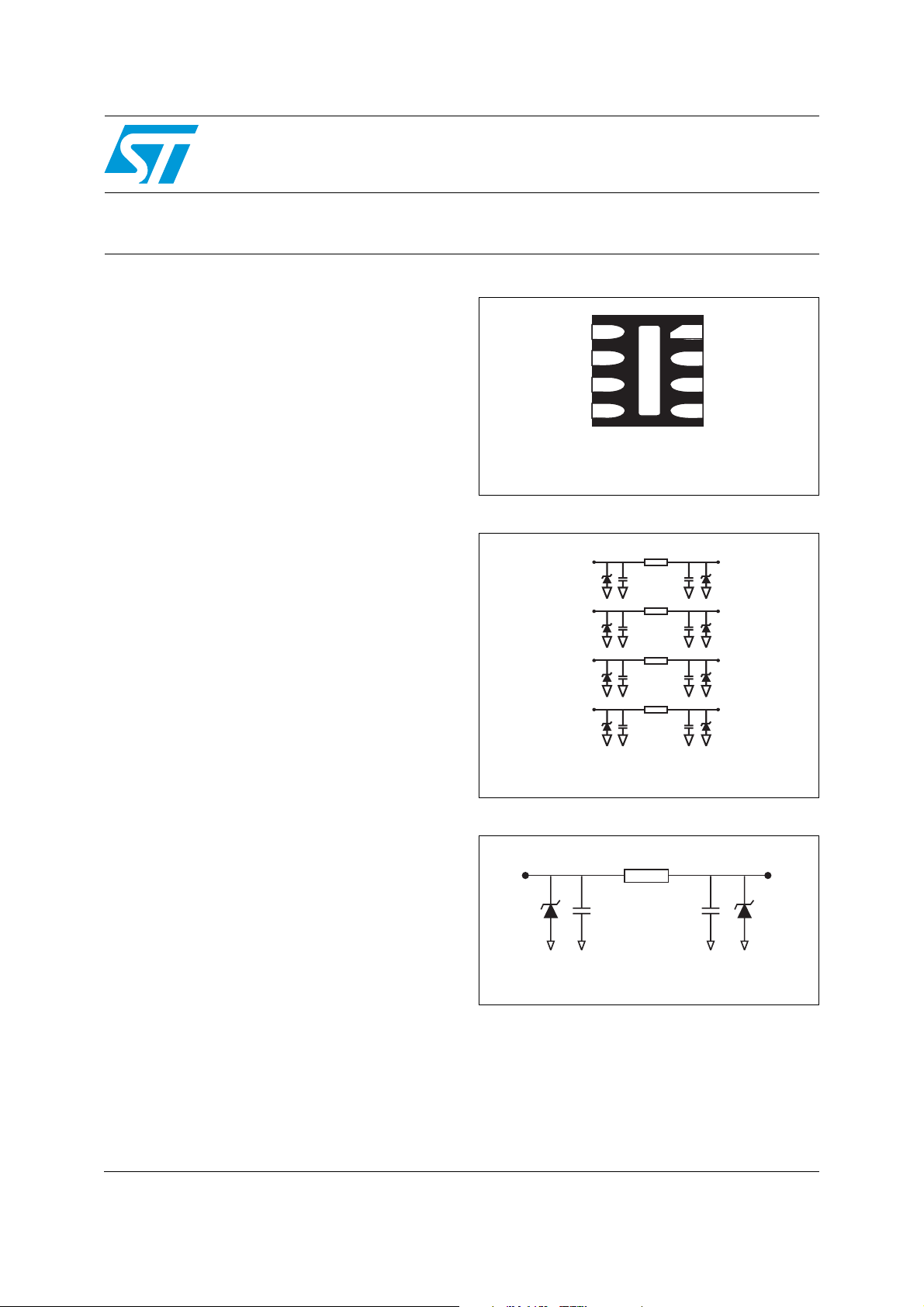
EMIF04-1005M8
4-line IPAD™
8
7
6
5
Micro QFN 1.7 mm x 1.5 mm
GND
GND
(bottom view)
Figure 1. Pin configuration (top view)
1 Input Output 8
1
2
3
4
Complies with following standards:
■ IEC 61000-4-2 level 4 input pins
– 15 kV (air discharge)
– 8 kV (contact discharge)
■ MIL STD 883G - Method 3015-7 Class 3B
(all pins)
Applications
Where EMI filtering in ESD sensitive equipment is
required:
■ LCD and camera for mobile phones
■ Computers and printers
■ Communication systems
■ MCU boards
Description
The EMIF04-1005M8 is a 4-line highly integrated
device designed to suppress EMI/RFI noise in all
systems exposed to electromagnetic interference.
This filter includes an ESD protection circuitry,
which prevents damage to the application when
subjected to ESD surges up to 15 kV on the input
pins.
2 Input
3 Input
4 Input
Figure 2. Basic cell configuration
Input
Typical line capacitance = 45 pF @ 0 V
TM: IPAD is a trademark of STMicroelectronics
100 Ω
Output 7
Output 6
Output 5
Output
January 2009 Rev 5 1/10
www.st.com
10
Characteristics EMIF04-1005M8
1 Characteristics
Table 1. Absolute ratings (limiting values at T
= 25 °C unless otherwise specified)
amb
Symbol Parameter Value Unit
V
T
T
Table 2. Electrical characteristics (T
ESD IEC 61000-4-2, air discharge
PP
ESD IEC 61000-4-2, contact discharge
Junction temperature 125 °C
T
j
Operating temperature range -40 to + 85 °C
op
Storage temperature range -55 to +150 °C
stg
Symbol Parameter
V
I
V
V
R
I
R
C
BR
RM
RM
CL
PP
I/O
line
Breakdown voltage
Leakage current @ V
RM
Stand-off voltage
Clamping voltage
Dynamic resistance
d
Peak pulse current
Series resistance between Input & Output
Input capacitance per line
amb
= 25 °C)
I
I
F
V
BR
V
V
RM
CL
I
RM
I
R
I
PP
15
15
V
F
V
Symbol Test conditions Min. Typ. Max. Unit
kV
V
BR
V
F
I
RM
R
I/O
C
line
IR = 1 mA 6 8 10 V
IF = 10 mA 0.5 1.0 1.5 V
VRM = 3 V per line 200 nA
Tolerance ± 10% 90 100 110 Ω
V
= 0 V dc, V
LINE
= 30 mV, F = 1 MHz 38 45 52 pF
OSC
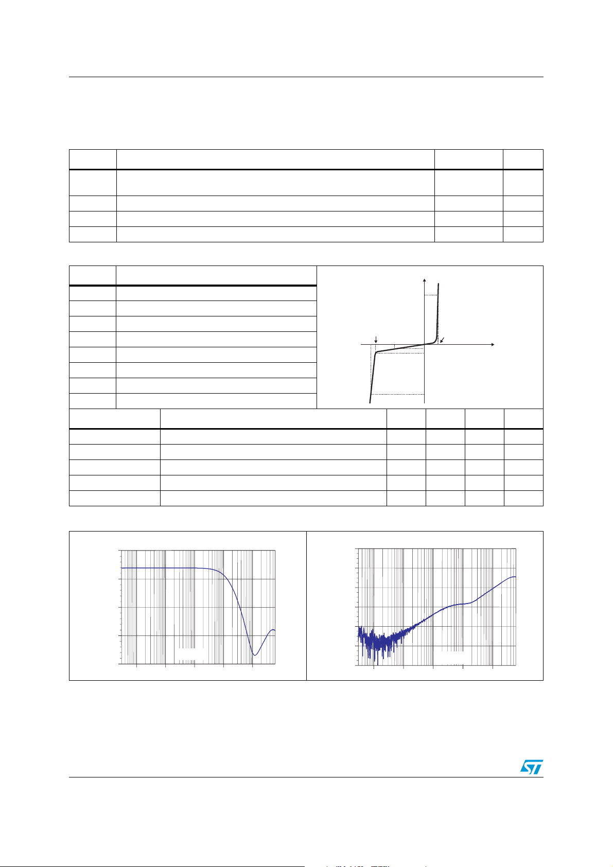
Figure 3. S21 attenuation measurement Figure 4. Analog cross talk measurements
dB
0.00
-10.00
-20.00
-30.00
F (Hz)
-40.00
100.0k 1.0M 10.0M 100.0M 1.0G
0.00
-20.00
-40.00
-60.00
-80.00
-100.00
-120.00
dB
F (Hz)
100.0k 1.0M 10.0M 100.0M 1.0G
2/10
EMIF04-1005M8 Ordering information scheme
Figure 5. ESD response to IEC 61000-4-2
(+15 kV air discharge) on one input
(V
) and on one output (V
in
out
)
Figure 6. ESD response to IEC 61000-4-2
(- 15 kV air discharge) on one input
(Vin) and on one output (V
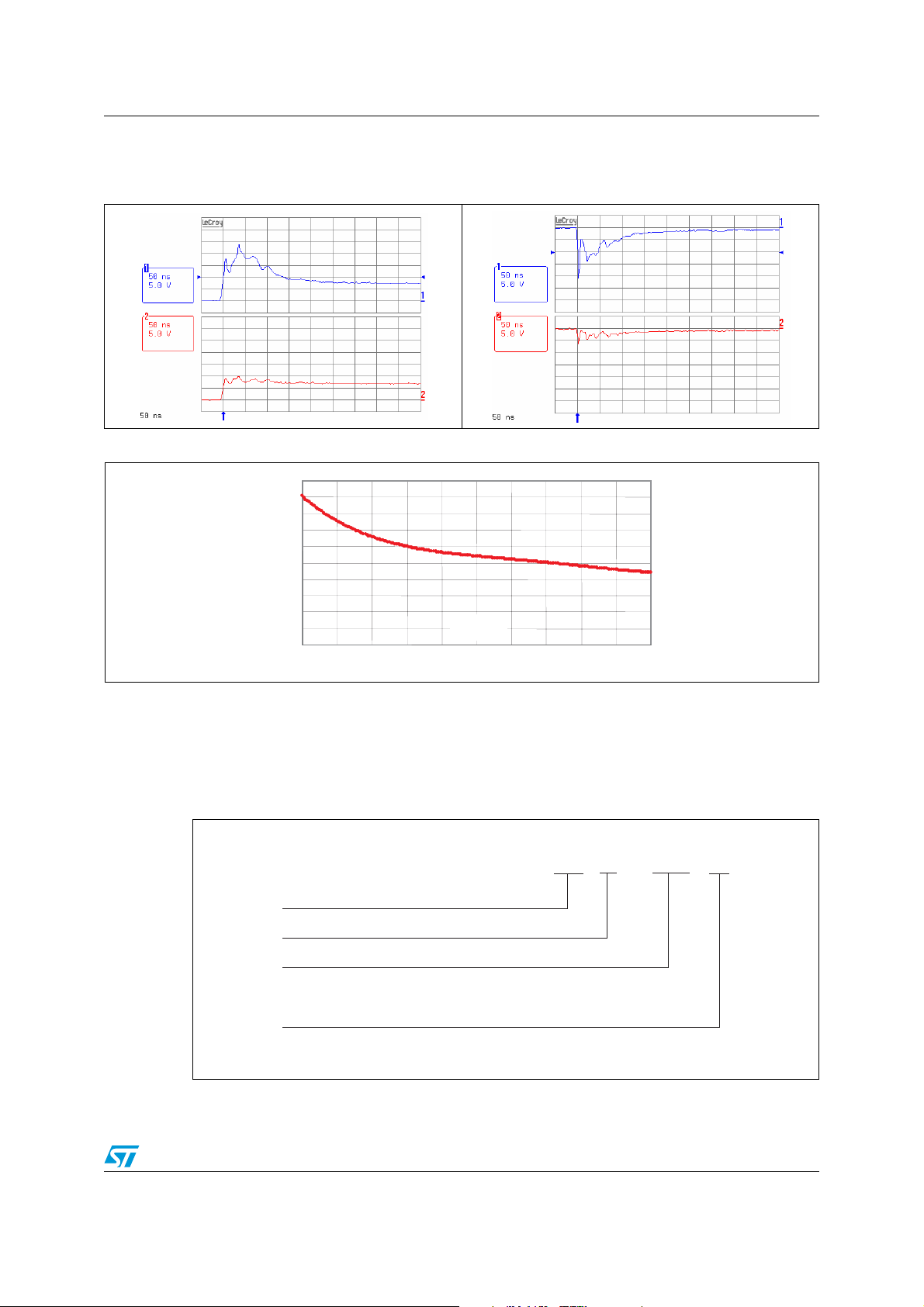
Figure 7. Line capacitance versus reverse voltage applied (typical value)
C
(pF)
LINE
50.00
45.00
40.00
35.00
30.00
25.00
20.00
15.00
10.00
V
5.00
0.00
0123 45
LINE
(V)
out
)
2 Ordering information scheme
Figure 8. Ordering information scheme
EMI Filter
Number of lines
Information
x = resistance value (Ohms)
z = capacitance value / 10(pF)
Package
Mx = Micro QFN x leads
3/10
EMIF yy - xxx z Mx
 Loading...