

3-line IPAD™, EMI filter including ESD protection
Features
■ EMI symmetrical (I/O) low-pass filter
■ high efficiency in EMI/ESD protection
■ lead-free package
■ very thin package
■ high reliability offered by monolithic integration
■ high reduction of parasitic elements through
integration and wafer level packaging
Complies with the following standards
■ IEC 61000-4-2 level 4:
– ± 15 kV (air discharge)
– ± 8 kV (contact discharge)
■ IEC 61000-4-2 level 1:
– ± 2 kV (air discharge)
– ± 2 kV (contact discharge)
Applications
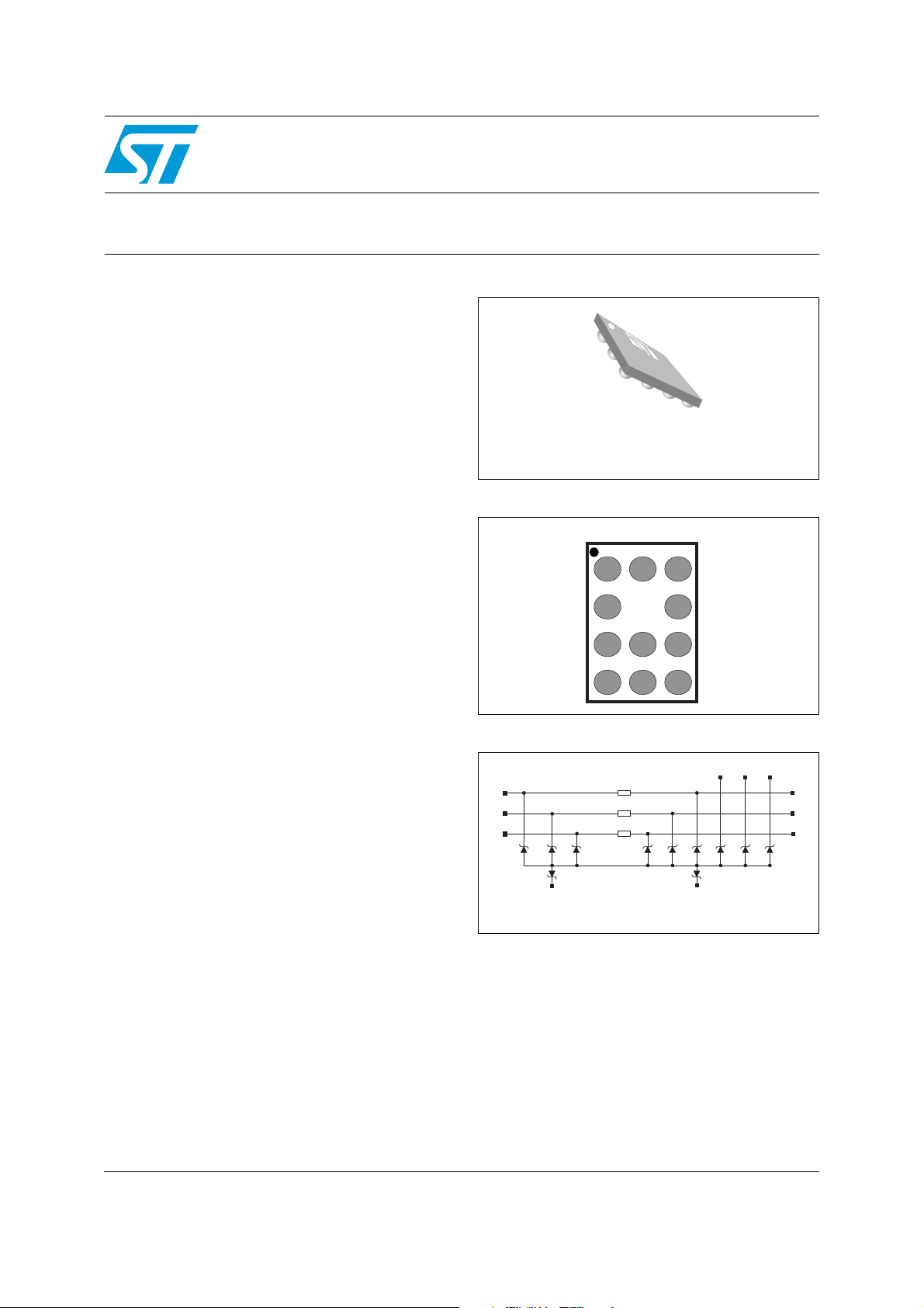
EMIF03-SIM04F3
Lead-free Flip-Chip package
(11 bumps)
Figure 1. Pin configuration (bump side)
1 2 3
A
B
C
D
Where EMI filtering in ESD sensitive equipment is
required:
■ mobile phones and communication systems
■ computers, printers and MCU Boards
Description
The EMIF03-SIM04F3 Flip Chip is a low
capacitance EMI filter designed to suppress
EMI/RFI noise in all systems subjected to
Figure 2. Configuration
D1 D3D2
A1
B1
C1
A2
GND
A2 and C2 bumps must be connected together on the PCB
100 Ω
R1
47 Ω
R2
100 Ω
R3
C2
GND
electromagnetic interference.
This filter includes ESD protection circuitry, which
prevents damage to the protected device when
subjected to ESD surges up to 15 kV.
TM: IPAD is a trademark of STMicroelectronics.
October 2010 Doc ID 17053 Rev 2 1/7
A3
B3
C3
www.st.com
7
Electrical characteristics EMIF03-SIM04F3
1 Electrical characteristics
Table 1. Absolute maximum ratings (T
Symbol Parameter Value Unit
Internal pins (A1, B1, C1):
ESD discharge IEC 61000-4-2, level 1, air discharge
V
PP
P
d
T
op
ESD discharge IEC 61000-4-2, level 1, contact discharge
External pins (A3, B3, C3, D1, D2 and D3):
ESD discharge IEC 61000-4-2, level 4, air discharge
ESD discharge IEC 61000-4-2, level 4, contact discharge
Line resistance power dissipation at 70 °C 60 mW
Operating temperature range - 40 to + 85 °C
amb
= 25 °C)
±2
±2
±15
±15
kV
T
Storage temperature range - 55 to 150 °C
stg
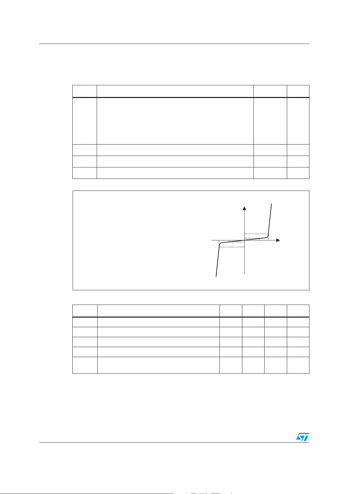
Figure 3. Electrical characteristics (definitions)
I
Symbol Parameter
V = Breakdown voltage
BR
I = Leakage current @ V
RM RM
R = Series resistance
I/O
between input and output
C = Line capacitance
line
Table 2. Electrical characteristics (T
amb
= 25 °C)
Symbol Test conditions Min. Typ. Max. Unit
V
BRIR
I
RM
R
1, R3
R
2
C
line
1. A2 and C2 bumps must be connected together on the printed circuit board
= 1 mA 6 V
VRM = 3 V per line 50 200 nA
Tolerance ± 20% 80 100 120 Ω
Tolerance ± 20% 37.6 47 56.4 Ω
V
= 0 V, V
line
(measured under zero light conditions)
= 30 mV, F = 1 MHz
osc
(1)
IR
IRM
VRMVBR
IRM
IR
V
V
BRVRM
81012pF
2/7 Doc ID 17053 Rev 2
EMIF03-SIM04F3 Electrical characteristics
Figure 4. S21 (dB) attenuation measurement
B3 - B1
S21 (dB)
0.00
-
-
-
10.00
-20.00
-
-
-30.00
-
-
-40.00
-
-
-50.00
-
-
100.0k 1.0M 10.0M 100.0M 1.0G
F (Hz)
1.0G
Figure 6. ESD response to IEC 61000-4-2
(+15 kV air discharge) on one line
20 V/Div
IN
C2
10 V/Div
OUT
100 ns/dIV
Figure 5. S21 (dB) analog crosstalk
measurements C3 - A1
S21 (dB)
0.00
-20.00
-
-40.00
-
-60.00
-
-80.00
-
100.00
-
100.0k 10.0M 100.0M 1.0G
1.0M
F (Hz)
Figure 7. ESD response to IEC 61000-4-2
(-15 kV air discharge) on one line
C2
10 V/Div
IN
100 ns/Div
C3
OUT
C3
Figure 8. Digital crosstalk measurement
1 V/Div
IN
C2
500 mV/Div
OUT
C3
100 ns/dIV
20 ns/Div
20 ns/Div
10 V/Div
100 ns/Div
Doc ID 17053 Rev 2 3/7
 Loading...