

ST EMIF03-SIM02M8 User Manual
EMIF03-SIM02M8
3 line IPAD™, EMI filter for SIM card applications
Features
■ SIM card EMI low-pass filter
■ High efficiency in EMI filtering
■ Very low PCB space consumption:
1.7 mm x 1.5 mm
■ Very thin package: 0.6 mm max
■ High efficiency in ESD suppression on external
pins (IEC 61000-4-2 level 4).
■ High reliability offered by monolithic integration
■ High reduction of parasitic elements through
integration and wafer level packaging.
■ Lead free package
■ Easy layout and flexibility thanks to I/O
topology
■ Low clamping voltage
Complies with following standards
■ IEC 61000-4-2 level 4 external pins
– 15 kV (air discharge)
– 8 kV (contact discharge)
■ IEC 61000-4-2 level 2 internal pins
– 2 kV (air discharge)
– 2 kV (contact discharge)
■ MIL STD 883G - Method 3015-7 Class 3A (all
pins)
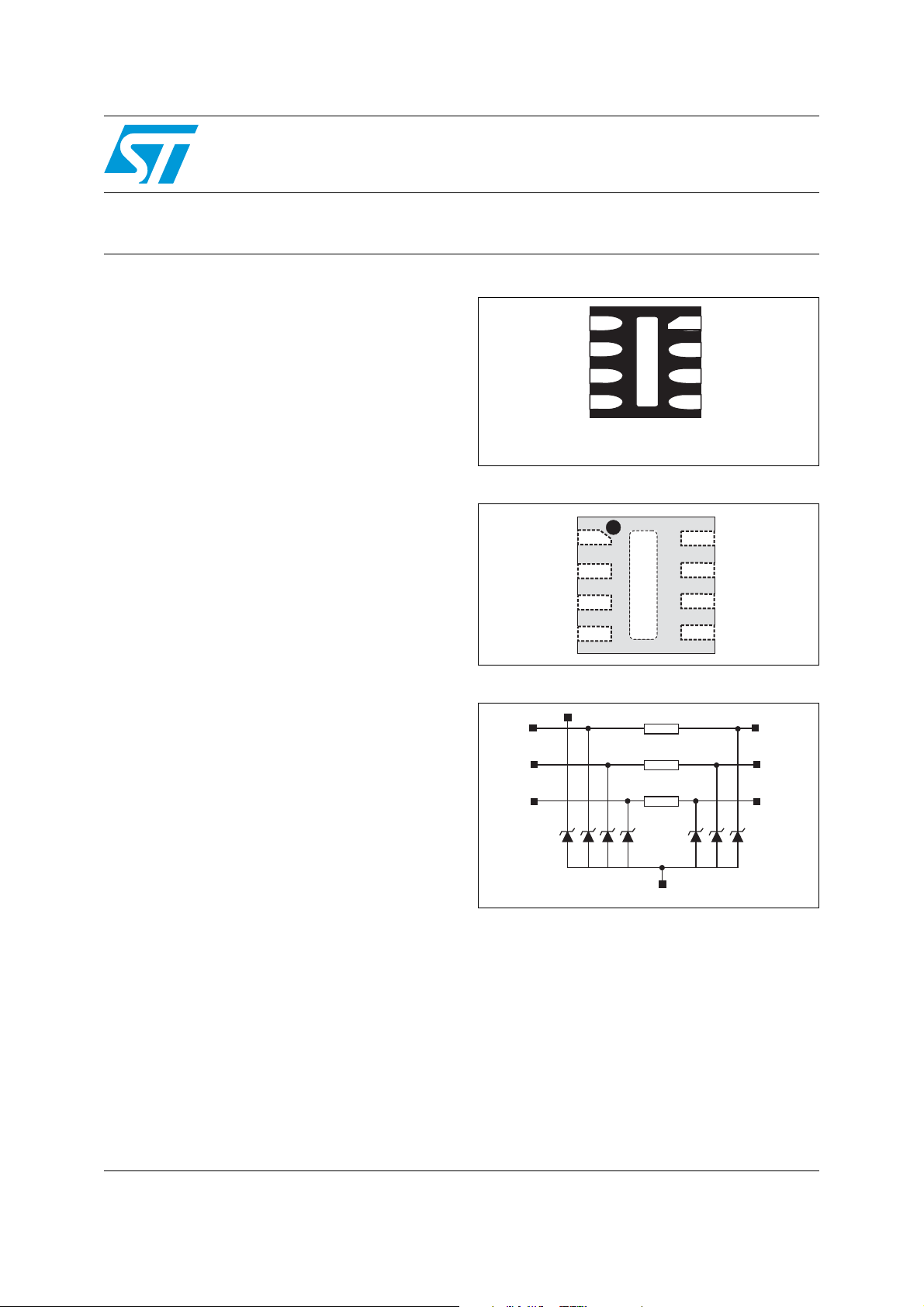
8
7
6
5
GND
GND
11
2
3
4
Micro QFN 1.7 mm x 1.5 mm
(bottom view)
Figure 1. Pin configuration (top view)
RST
CLK
Data
Vcc
in
in
in
GND
Vcc
RST
CLK
Data
EXT
EXT
EXT
Figure 2. Device configuration
RST in
CLK in
Data in
Vcc
100 Ω
R1
47 Ω
R2
100 Ω
R3
RST ext
CLK ext
Data ext
Applications
Maximum line capacitance = 20 pF
GND
Where EMI filtering in ESD sensitive equipment is
required:
■ Keyboard for mobile phones
■ Computers and printers
■ Communication systems
■ MCU boards
Description
The EMIF03-SIM02M8 is a 3 line highly
integrated device designed to suppress EMI/RFI
noise in all systems exposed to electromagnetic
interference.
This filter includes ESD protection circuitry, which
prevents damage to the application when
subjected to ESD surges up to 15 kV on the
TM: IPAD is a trademark of STMicroelectronics
October 2007 Rev 1 1/10
external pins.
www.st.com
Characteristics EMIF03-SIM02M8
1 Characteristics
Table 1. Absolute ratings (limiting values at T
= 25 °C unless otherwise specified)
amb
Symbol Parameter Value Unit
Internal pins
ESD discharge IEC 61000-4-2 air discharge
ESD discharge IEC 61000-4-2 contact discharge
V
External pins and V
PP
ESD discharge IEC 61000-4-2 air discharge
CC
ESD discharge IEC 61000-4-2 contact discharge
2
2
15
8
All pins
MIL STD 883G - Method 3015-7 Class 3A (human body model)
Junction temperature 125 °C
T
j
T
T
Table 2. Electrical characteristics (T
Operating temperature range -40 to + 85 °C
op
Storage temperature range -55 to +150 °C
stg
Symbol Parameter
V
I
V
V
I
R
C
Breakdown voltage
BR
Leakage current @ V
RM
Stand-off voltage
RM
Clamping voltage
CL
Peak pulse current
PP
Series resistance between input and output
I/O
Input capacitance per line
line
RM
amb
= 25 °C)
I
I
F
V
BR
V
V
RM
CL
I
RM
I
R
I
PP
4
V
F
V
Symbol Test conditions Min. Typ. Max. Unit
V
I
R
1
R
C
IR = 1 mA 6 7.9 V
BR
VRM = 3 V 0.2 µA
RM
, R3Tolerance ± 20% 100 Ω
Tolerance ± 20% 47 Ω
2
VR= 0 V, F = 1 MHz, V
line
= 30 mV 17 20 pF
OSC
kV
2/10
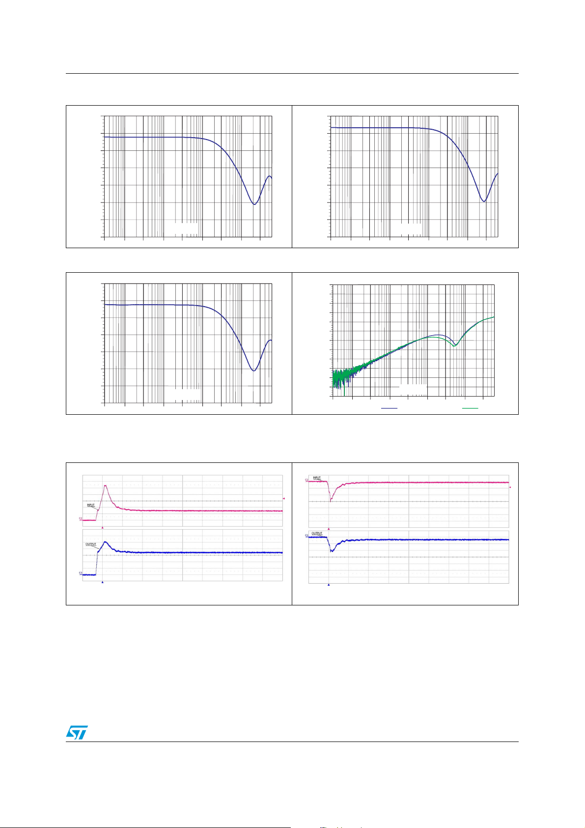
EMIF03-SIM02M8 Characteristics
Figure 3. S21(db) attenuation (RST line) Figure 4. S21(db) attenuation (CLK line)
dB
0.00
-5.00
-10.00
-15.00
-20.00
-25.00
-30.00
F (Hz)
-35.00
300.0k 1.0M 3.0M 10.0M 30.0M 100.0M 300.0M 1.0G 3.0G
dB
0.00
-5.00
-10.00
-15.00
-20.00
-25.00
-30.00
-35.00
300.0k 1.0M 3.0M 10.0M 30.0M 100.0M 300.0M 1.0G 3.0G
F (Hz)
Figure 5. S21(db) attenuation (DATA line) Figure 6. Analog cross talk measurements
dB
0.00
-5.00
-10.00
-15.00
-20.00
-25.00
-30.00
F (Hz)
-35.00
300.0k 1.0M 3.0M 10.0M 30.0M 100.0M 300.0M 1.0G 3.0G
Figure 7. ESD response to IEC 61000-4-2
(+15 kV air discharge) applied to
external pin
Figure 8. ESD response to IEC 61000-4-2
dB
0.00
-10.00
-20.00
-30.00
-40.00
-50.00
-60.00
-70.00
-80.00
-90.00
-100.00
-110.00
-120.00
300.0k 1.0M 3.0M 10.0M 30.0M 100.0M 300.0M 1.0G 3.0G
ClkIn- RstExt DataIn-Rst/Clk
F (Hz)
(-15 kV air discharge) applied to
external pin
5 V/div
2 V/div
200 ns/div
5 V/div
2 V/div
200 ns/div
3/10
 Loading...