

ST EMIF02-SPK01C2 User Manual
IPAD™
Main product characteristics
Where EMI filtering in ESD sensitive equipment is
required:
■ Mobile phones and communication systems
■ Computers and printers and MCU Boards
Description
The EMIF02-SPK01C2 is a highly integrated
device designed to suppress EMI/RFI noise in all
systems subjected to electromagnetic
interference. The Flip-Chip packaging means the
package size is equal to the die size.
This filter includes ESD protection circuitry, which
prevents damage to the application when it is
subjected to ESD surges up to 15 kV.
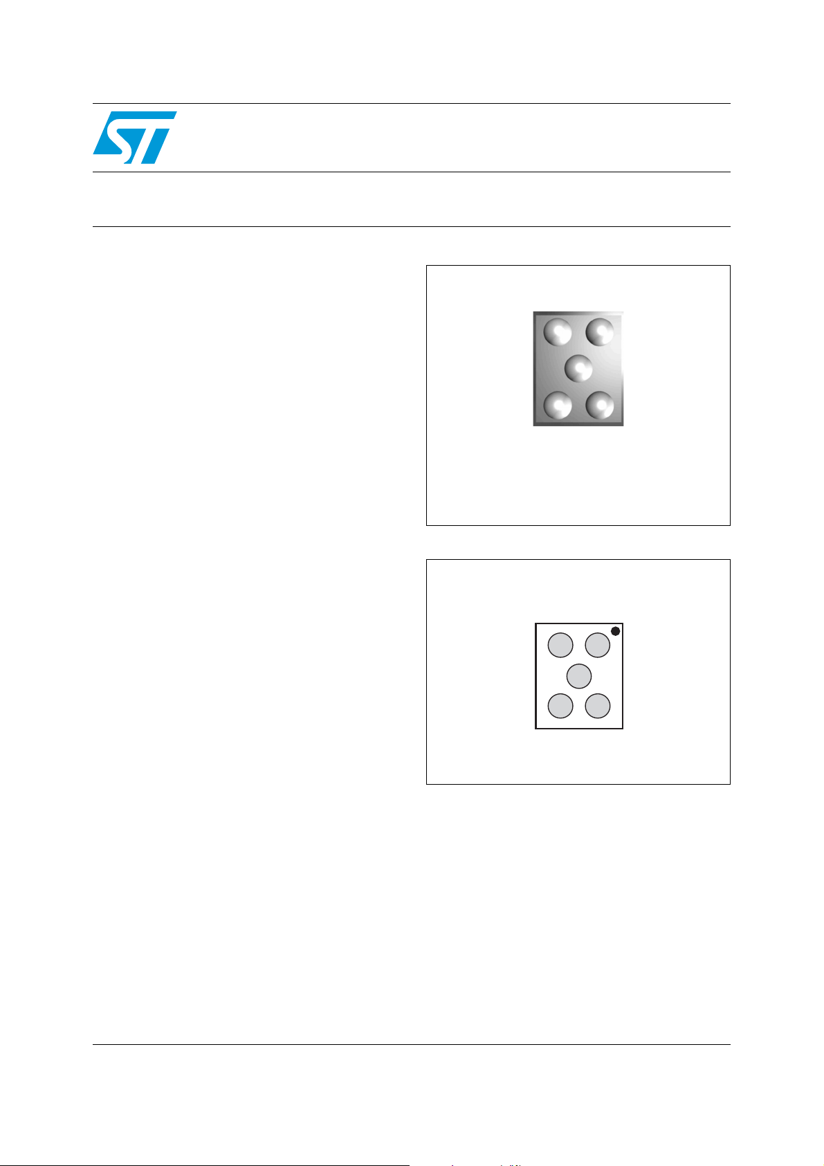
EMIF02-SPK01C2
2 line EMI filter and ESD protection
Coated Flip-Chip package
(about 20 times real size)
Pin configuration (Bump side)
Benefits
■ EMI symmetrical (I/O) low-pass filter
■ High efficiency EMI filter (-33 dB @ 900 MHz)
■ Very low PCB space consumption:
1.07 mm x 1.47 mm
■ Very thin package: 0.695 mm
■ Coating resin on back side and lead free
package
■ High efficiency in ESD suppression
■ High reliability offered by monolithic integration
■ High reduction of parasitic elements through
integration and wafer level packaging.
132
I1
I2
GND
O2
O1
A
B
C
Complies with following standards:
IEC 61000-4-2
level 4 input pins 15 kV (air discharge)
8 kV (contact discharge
level 1 output pins 2 kV (air discharge)
2 kV (contact discharge
MIL STD 883G - Method 3015-7 Class 3
January 2007 Rev 1 1/7
www.st.com
Characteristics EMIF02-SPK01C2
1 Characteristics
Figure 1. Basic cell configuration
Low-pass Filter
Input
Output
Ri/o = 10
Ω
Cline = 200 pF
GND GND GND
Table 1. Absolute ratings (limiting values)
Symbol Parameter Value Unit
T
T
op
T
stg
Table 2. Electrical characteristics (T
Maximum junction temperature 125 °C
j
Operating temperature range -40 to +85 °C
Storage temperature range -55 to +150 °C
= 25° C)
amb
Symbol Parameters
V
I
V
V
Breakdown voltage
BR
Leakage current @ V
RM
Stand-off voltage
RM
Clamping voltage
CL
R
Dynamic impedance
d
RM
VCL
VRMVBR
I
IR
IRM
I
PP
IRM
IR
VBRVRM
VCL
V
I
Peak pulse current
PP
R
C
Series resistance between input and output
I/O
Input capacitance per line
line
Symbol Test conditions Min Typ Max Unit
V
BR
I
RM
R
I/O
C
line
IR = 1 mA 6 8 V
VRM = 3 V per line 500 nA
Tolerance ±20% 10 Ω
VR = 0 V 200 pF
2/7
IPP
EMIF02-SPK01C2 Characteristics
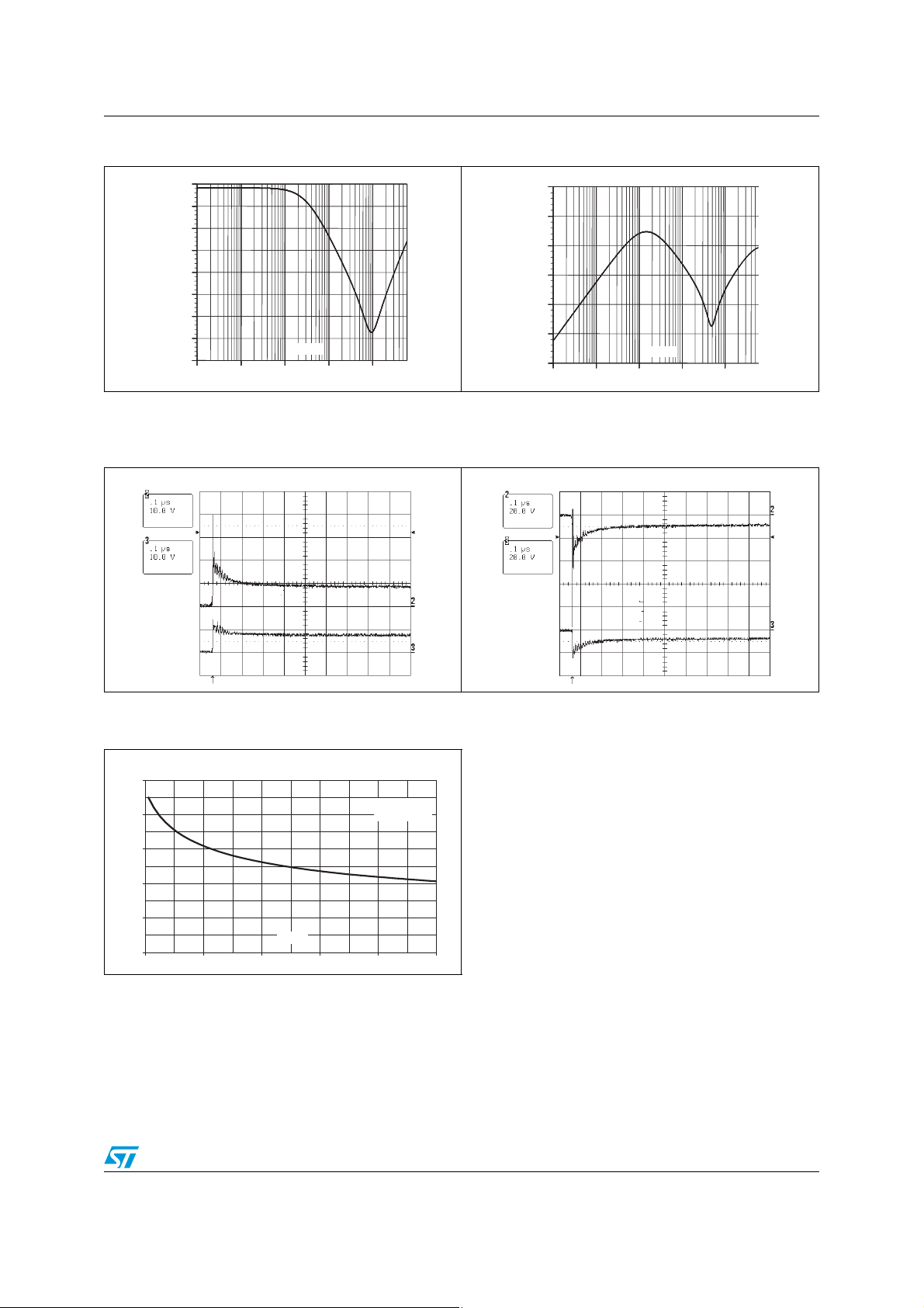
Figure 2. S21 (dB) attenuation measurement Figure 3. Analog crosstalk measurement
dB
0.00
-
-5.00
-
-10.00
-
-15.00
-
-20.00
-
-25.00
-
-30.00
-35.00
-40.00
100.0k 1.0M 10.0M 100.0M 1.0G
1.0M
F (Hz)
Figure 4. ESD response to IEC 61000-4-2
(+15 kV air discharge) on one
input V
and one output V
in
out
Figure 5. ESD response to IEC 61000-4-2
dB
0.00
-10.00
-
-20.00
-
-30.00
-
-40.00
-
-50.00
-
-60.00
-
100.0k 1.0M 10.0M 100.0M 1.0G
F (Hz)
(- 15 kV air discharge) on one
input V
and one output V
in
out
Figure 6. Line capacitance versus applied
voltage
C(pF)
250
F=1MHz
V
=30mV
osc
200
150
100
50
V (V)
0
012345
R
Tj=25°C
RMS
3/7
 Loading...