Single line IPAD™, EMI filter including ESD protection
Features
■ High density capacitor
■ 1 line low-pass-filter
■ Lead-free package
■ High efficiency in EMI filtering
■ Very low PCB space consumtion
■ Very thin package: 0.65 mm
■ High efficiency in ESD suppression
(IEC 61000-4-2 level 4)
■ High reliability offered by monolithic integration
■ High density capacitor technology
Complies with the following standards
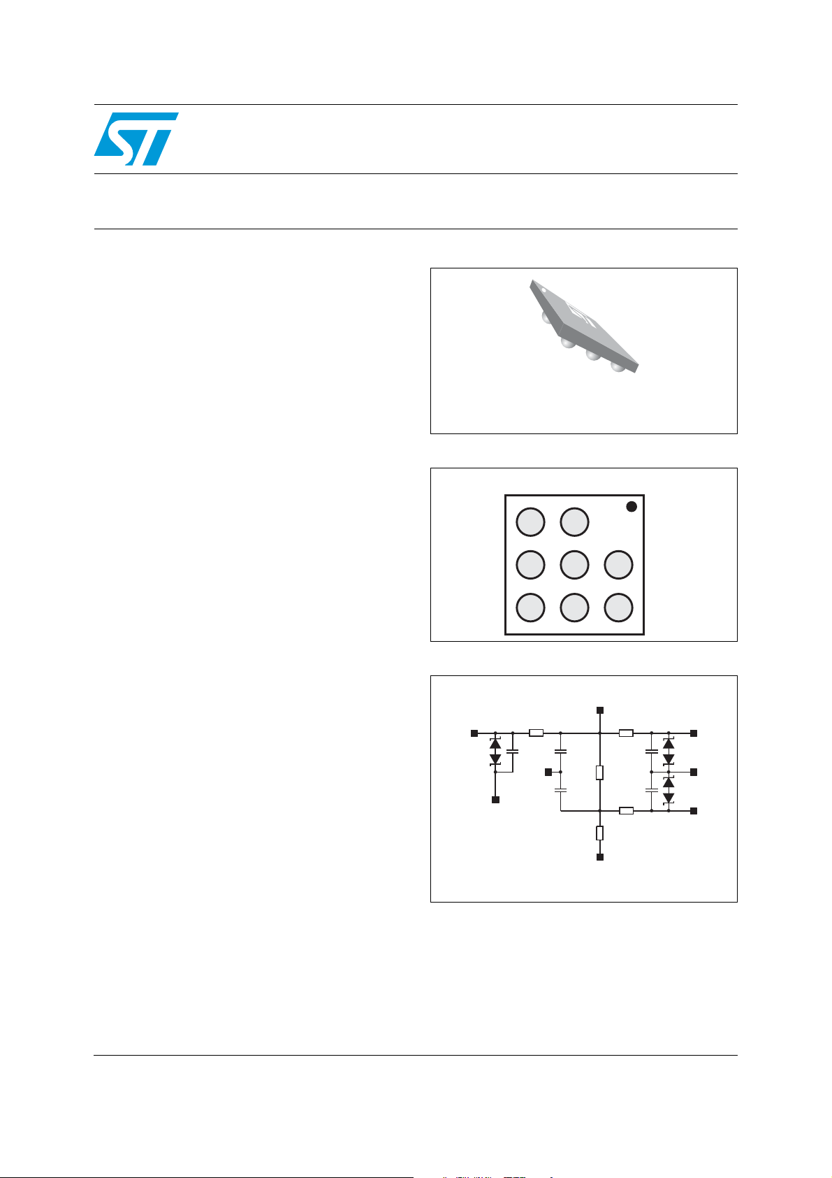
EMIF01-SMIC01F2
Flip Chip
(8 bumps)
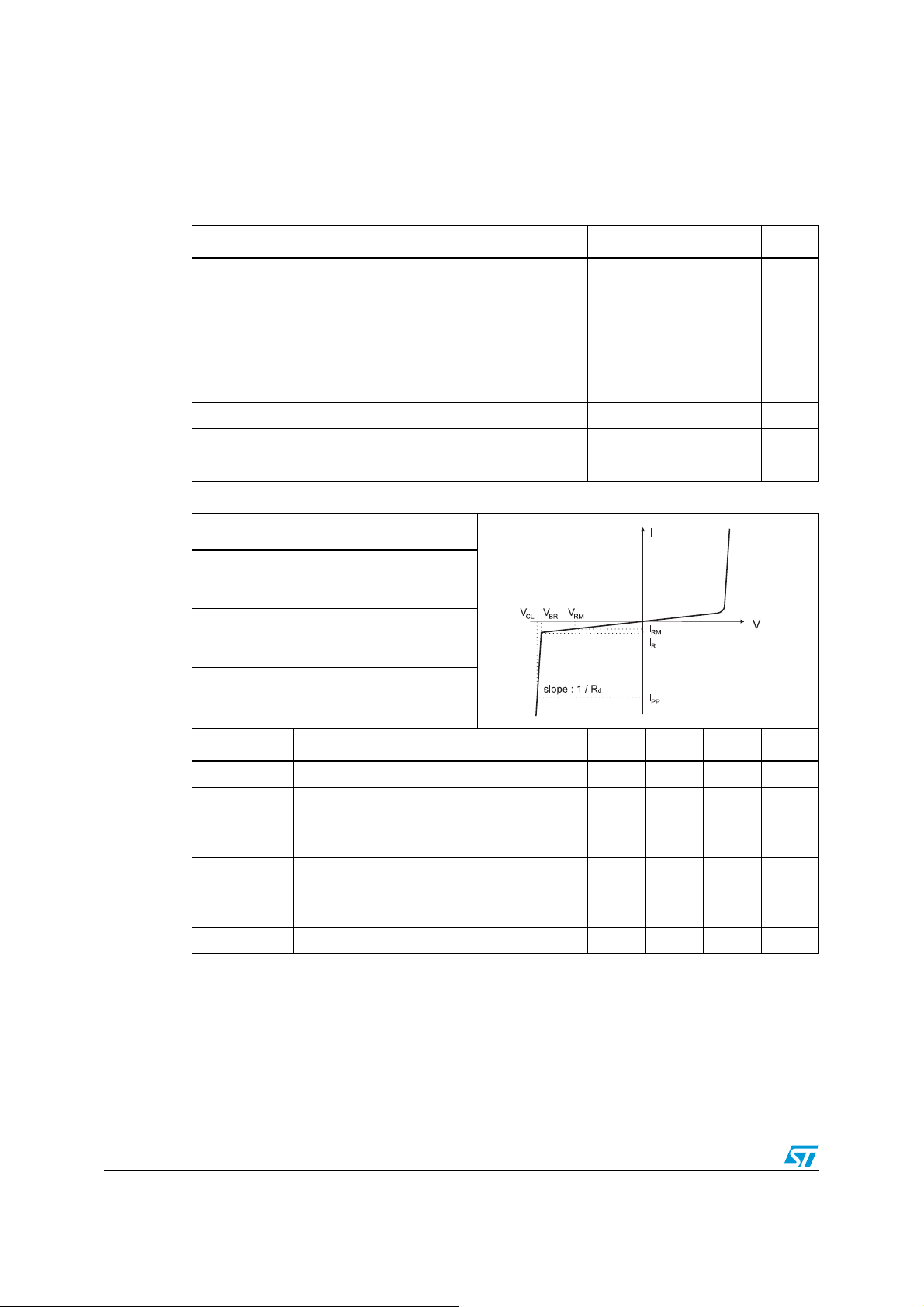
Figure 1. Pin configuration (bump side)
32
1
A
■ IEC 61000-4-2 level 4, on output pins
– 15 kV (air discharge)
– 8 kV (contact discharge
■ IEC 61000-4-2 Level 1, on input pins
– 2 kV (air and contact discharge)
Application
■ Single ended microphone in mobile phones
and portable devices
Description
The EMIF01-SMIC01F2 is a highly integrated
device designed to suppress EMI/RFI noise for
microphone line filtering.
The EMIF01-SMIC01F2 Flip Chip packaging
means the package size is equal to the die size.
That is why EMIF01-SMIC01F2 is a very small
device.
Additionally, this filter includes ESD protection
circuitry which prevents damage to the appication
when subjected to ESD surges up to 15 kV.
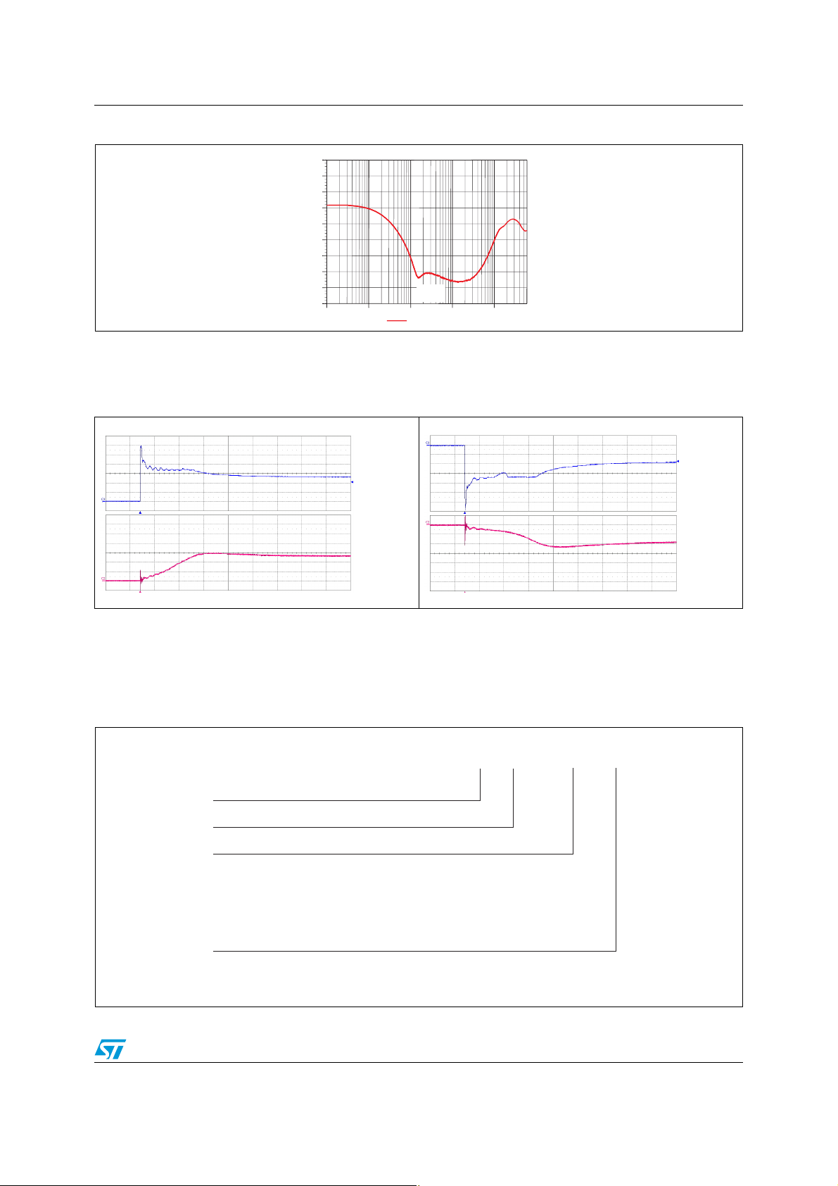
Figure 2. Schematic
C3
B2, B3, C2 are GND bumps
R1
C1
B2
B3
B
C
A3
R2
C2
C5
C3
R3
C4
R4
R5
A2
B1
C2
C1
TM: IPAD is a trademark of STMicroelectronics
April 2008 Rev 2 1/7
www.st.com
7

Characteristics EMIF01-SMIC01F2
1 Characteristics
Table 1. Absolute maximum matings (T
Symbol Parameter and test conditions Value Unit
Output lines (C3)
ESD discharge IEC61000-4-2, air discharge
ESD discharge IEC61000-4-2, contact discharge
V
PP
Input lines (A3, A2, B1, C1)
ESD discharge IEC61000-4-2, air discharge
ESD discharge IEC61000-4-2, contact discharg
Maximum junction temperature 125 °C
T
j
T
T
Table 2. Electrical characteristics (T
Symbol Parameter
Operating temperature range - 40 to + 85 °C
op
Storage temperature range - 55 to + 150 °C
stg
amb
= 25 °C)
amb
= 25 °C)
15
8
kV
2
2
V
I
V
V
Breakdown voltage
BR
Leakage current @ V
RM
Stand-off voltage
RM
Clamping voltage
CL
Dynamic impedance
R
d
I
Peak pulse current
PP
RM
Symbol Test conditions Min. Typ. Max. Unit
V
BR
I
RM
C1, C2, C3, C4,
C
5
, R
R
1
, R3, R4 Tolerance ± 5% 2.2 kΩ
R
2
IR = 1 mA 14 V
VRM = 3 V per line 0.5 µA
V
= 0 V, V
LINE
Tolerance ± 20%
V
= 0 V, V
LINE
Tolerance ± 20%
Tolerance ± 5% 50 Ω
5
= 30 mV, F = 1 MHz,
OSC
= 30 mV, F = 1 MHz,
OSC
1nF
150 pF
2/7

EMIF01-SMIC01F2 Ordering information scheme
Figure 3. Filtering measurements
dB
0.00
-10.00
-20.00
-30.00
-40.00
-50.00
-60.00
-70.00
-80.00
-90.00
100.0k 1.0M 10.0M 100.0M 1.0G
C3-B1 line
Figure 4. ESD response to IEC 61000-4-2
(+15 kV air discharge) on one
output line
F (Hz)
Figure 5. ESD response to IEC 61000-4-2
(-15 kV air discharge) on one output
line
Vin=5V/d
Vout=5V/d
1µs/d
2 Ordering information scheme
Figure 6. Ordering information scheme
EMIF yy - xxx zz Fx
EMI Filter
Number of lines
Information
x = resistance value (Ohms)
z = capacitance value / 10(pF)
or
3 letters = application
2 digits = version
Vin=5V/d
Vout=5V/d
1µs/d
Package
F = Flip Chip
x = 2: Lead-free, pitch = 500 µm, bump = 310 µm
3/7
 Loading...