

Wide-band, dual-path directional coupler with ISO port
Features
■ 50 Ω nominal input / output impedance
■ wide operating frequency range:
– 824 MHz-2170 MHz
■ low insertion loss (< 0.2 dB)
■ 37 dB typical coupling factor
■ high directivity (> 20 dB)
■ high ESD ruggedness
■ lead-free CSP package
■ Flip-Chip package
■ small footprint: 1700 x 1850 µm
■ very low profile (< 670 µm thickness)
Benefits
■ high RF performance
■ RF module size reduction
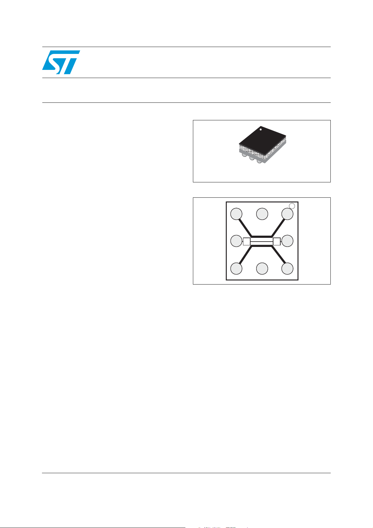
DCPL-WB-00C2
Lead-free Flip Chip (8 bumps)
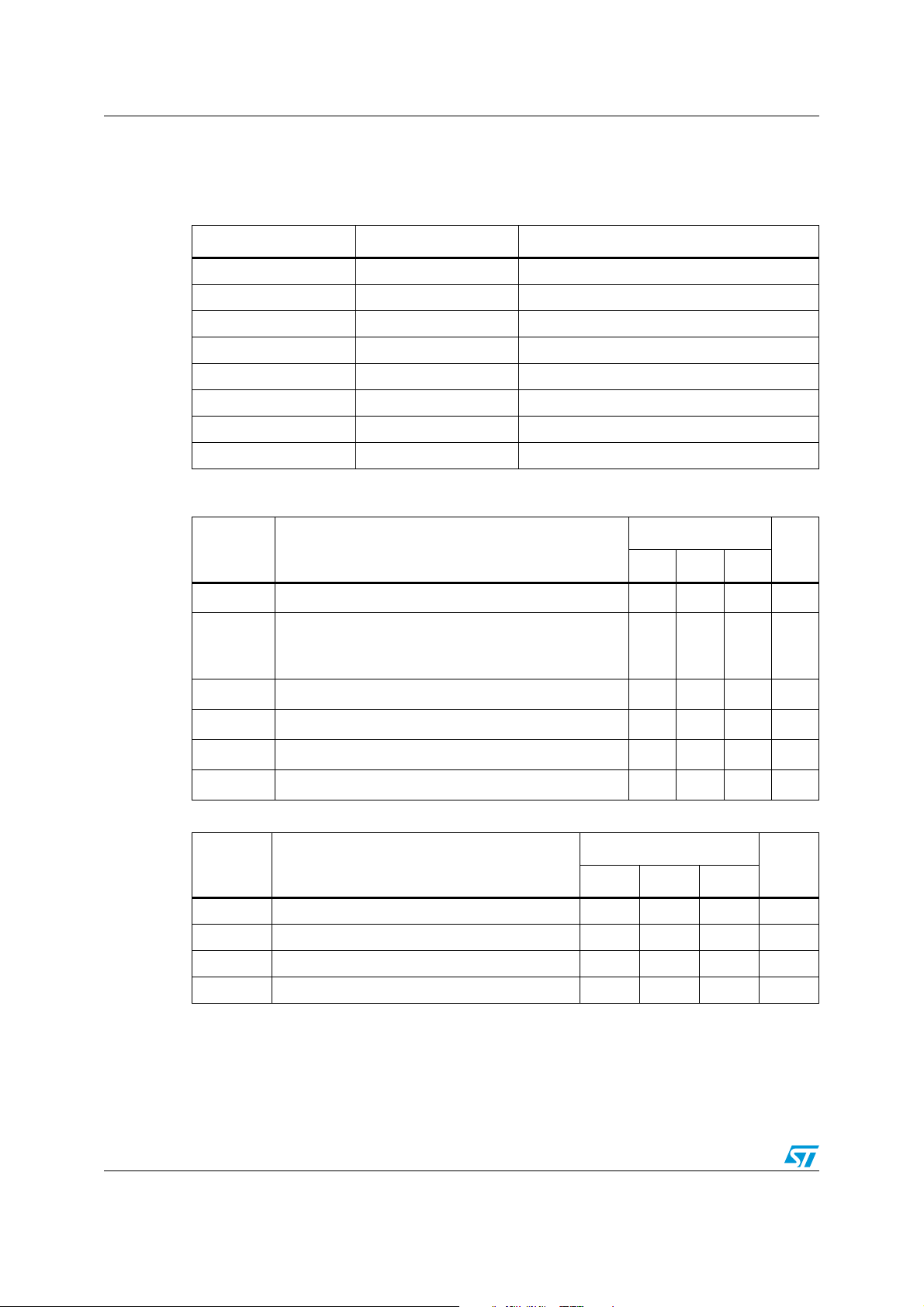
Figure 1. Pin configuration (bump view)
A1A2A3
LB Path
ISO
HB Path
B1B3
C1C2C3
CPL
Complies with the following standards:
■ IEC 61000-4-2 level 4:
– 15 kV (air discharge)
– 8 kV (contact discharge)
Applications
Multi-band equipment such as:
■ power amplifier module
■ front end module
■ GSM/WCDMA mobile phone
Description
The DCPL-WB-00C2 is a wide-band, dual-path
directional coupler designed to measure cell
phone transmission output power in
GSM/WCDMA applications. This dual-path CPL
has been customized for wide-band operating
frequencies (EGSM and CELL, PCS, DCS,
WCDMA band I) with less than 0.2 dB insertion
losses in the transmission bandwidth (824 MHz 1980 MHz).
This device is built with two different RF couplers
(one dedicated to LB, the other dedicated to HB)
sharing the same coupled and isolated ports.The
DCPL-WB-00C2 has been designed using
STMicroelectronics IPD (integrated passive
device) technology on non-conductive glass
substrate to optimize RF performance.
The device is delivered 100% tested in tape and
reel.
October 2010 Doc ID 17994 Rev 1 1/11
www.st.com
11
Characteristics DCPL-WB-00C2
1 Characteristics
Table 1. Device pin configuration
Bump Name Description
A1 Lbin LB coupler RF input
A2 GND RF ground
A3 Lbout LB coupler RF output
B1 CPLD Coupler port
B3 ISO Isolated port
C1 Hbin HB coupler RF input
C2 GND RF ground
C3 Hbout HB coupler output
Table 2. Absolute maximum rating (limiting values)
Value
Symbol Parameter
Min. Typ. Max.
Unit
P
IN
Input Power RF
(CW mode) - 36 dBm
IN
ESD ratings IEC 61000-4-2 (C = 150 pF, R = 330 Ω)
V
ESD (IEC)
V
ESD (HBM)
V
ESD (MM)
V
ESD (CDM)
T
OP
Table 3. Electrical characteristics - impedances (T
LB
LB
IN
IN
, LB
, LB
, HBIN, HB
OUT
, HBIN, HB
OUT
, air discharge
OUT
, contact discharge
OUT
Human body model, JESD22-A114-B, All I/O 2 - - kV
Machine model, JESD22-A115-A, All I/O 100 - - V
Charge device model, JESD22-C101-C, All I/O 500 - - V
Operating temperature -30 - +85 °C
Symbol Parameter
Z
Z
Z
OUT
Z
CPL
ISO
Nominal output impedance (LB and HB paths) - 50 - Ω
Nominal input impedance (LB and HB paths) - 50 - Ω
IN
Nominal coupled port impedance - 50 - Ω
Nominal isolated port impedance - 50 - Ω
±15
--kV
±8
= 25 °C)
amb
Value
Min. Typ. Max.
Unit
2/11 Doc ID 17994 Rev 1
DCPL-WB-00C2 Characteristics
Table 4. Electrical characteristics - LB path RF performance (T
Symbol Parameter Test condition
T
IL
Operating temperature -30 - +85 °C
OP
Frequency range
f
(bandwidth)
LB path insertion loss
LB
From 824 MHz
to 960 MHz
Min. Typ. Max.
824 - 960 MHz
Value
-0.10.2dB
amb
= 25 °C)
Unit
RL
CPLD
Ripple
DIR
LB path return loss
LB
LB coupling factor
LB
Coupling ripple in LB
LB
LB coupler directivity
LB
From 824 MHz
to 960 MHz
From 824 MHz
to 915 MHz
(824 to 849 MHz)
(880 to 915 MHz)
From 824 MHz
to 915 MHz
15 - - dB
32 - 37 dB
--0.5dB
22 - - dB
Table 5. Electrical characteristics - HB path RF performance (T
Symbol Parameter Test condition
T
IL
RL
CPLD
Operating temperature -30 - +85 °C
OP
Frequency range
f
(bandwidth)
HB path insertion loss
HB
HB path return loss
HB
HB coupling factor
HB
From 1710 MHz
to 2170 MHz
From 1710 MHz
to 2170 MHz
From 1710 MHz
to 1980 MHz
(1710 to 1785 MHz)
Ripple
Coupling ripple in HB
HB
(1850 to 1910 MHz)
(1920 to 1980 MHz)
DIR
HB coupler directivity
HB
From 1710 MHz
to 1980 MHz
Min. Typ. Max.
1710 - 1980 MHz
15 - - dB
29 - 34 dB
22 - - dB
Value
-0.10.2dB
--0.5dB
amb
= 25 °C)
Unit
Doc ID 17994 Rev 1 3/11
Characteristics DCPL-WB-00C2
1.1 RF measurement (on reference evaluation board)
Measurements done on reference evaluation board under 50 Ω, de-embedding at
DCPL-WB-00D3 bumps.
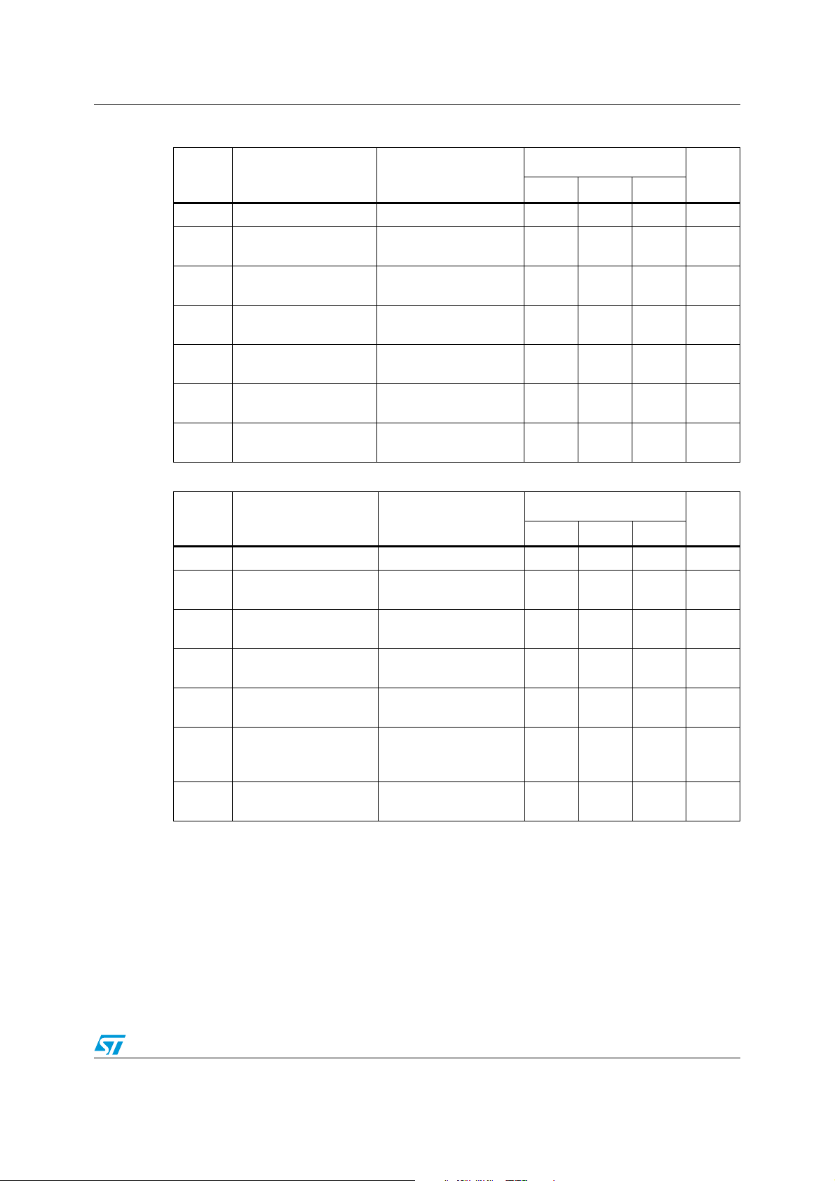
Figure 2. Low band path insertion loss
IL - LB (dB)
0.00
-0.05
-0.10
-0.15
F (MHz)
-0.20
800 820 840 860 880 900 920 940 960 980 1000
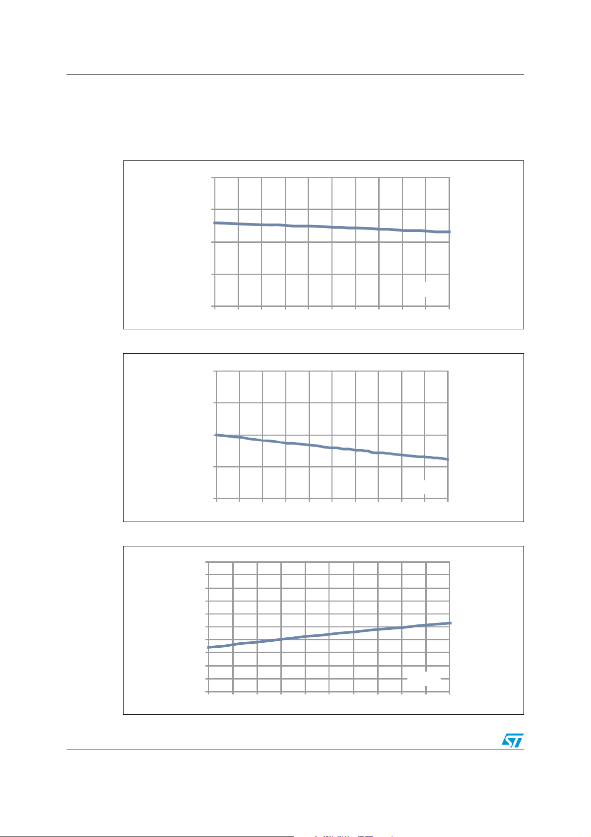
Figure 3. High band path insertion loss
IL - HB (dB)
0.00
-0.05
-0.10
-0.15
-0.20
1700 1750 1800 1850 1900 1950 2000 2050 2100 2150 2200
Figure 4. Low band path coupling factor
CPLD - LB (dB)
-30
-31
-32
-33
-34
-35
-36
-37
-38
-39
-40
800 820 840 860 880 900 920 940 960 980 1000
F (MHz)
F (MHz)
4/11 Doc ID 17994 Rev 1

DCPL-WB-00C2 Characteristics
001750180018501900195020002050210021502200
Figure 5. High band path coupling factor
CPLD - HB (dB)
-28
-29
-30
-31
-32
-33
-34
-35
36
--37
F (MHz)
-38
1700 1750 1800 1850 1900 1950 2000 2050 2100 2150 2200
Figure 6. Low band path directivity
DIR - LB (dB)
35
34
33
32
31
30
29
28
27
26
25
24
23
22
21
20
800 820 840 860 880 900 920 940 960 980 1000
F (MHz)
Figure 7. High band path directivity
DIR - LB (dB)
35
34
33
32
31
30
29
28
27
26
25
24
23
22
21
20
17
Doc ID 17994 Rev 1 5/11
F (MHz)

Characteristics DCPL-WB-00C2
Figure 8. Demo board description - layer 1
Copper pad diameter:
275 µm
Figure 9. Solder mask 1 + layer 1
Solder mask diameter:
375 µm
6/11 Doc ID 17994 Rev 1

DCPL-WB-00C2 Ordering information scheme
2 Ordering information scheme
Figure 10. Ordering information scheme
DCPL
Dual high directivity coupler
Wide band
Version
Package
C2 = Coated Flip Chip, bump size = 315 µm
– –
WB – 00 C2
Doc ID 17994 Rev 1 7/11

Package information DCPL-WB-00C2
3 Package information
● Epoxy meets UL94, V0
● Lead-free package
In order to meet environmental requirements, ST offers these devices in different grades of
ECOPACK
specifications, grade definitions and product status are available at: www.st.com
ECOPACK
®
packages, depending on their level of environmental compliance. ECOPACK®
®
is an ST trademark.
.
Figure 11. Package dimensions
685 µm
685 µm
B3
B3B3
600µm
A2A3
A2A2A3A3
1.7 mm
315 µm dia.
600µm
A1
A1A1
B1
B1B1
C1C2C3
C1C1C2C2C3C3
670 µm
1.85 mm
Figure 12. Footprint Figure 13. Marking
Copper pad diameter :
250 µm recommended, 300 µm max
Solder stencil opening: 330 µm
Solder mask opening recommendation:
340 µm min for 300 µm copper pad diameter
8/11 Doc ID 17994 Rev 1
Dot, ST logo
ECOPACK status
xx = marking
z = manufacturing
location
yww = datecode
(y = year ww = week)
xyx
wzw
DCPL-WB-00C2 Package information
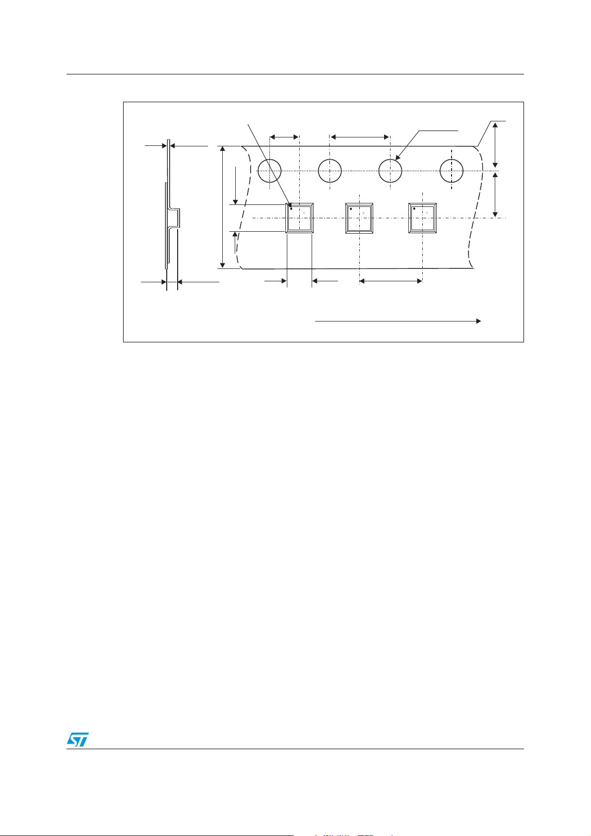
Figure 14. Flip-Chip tape and reel specifications
Dot identifying Pin A1 location
0.22
1.95
8.0
0.73
All dimensions are typical values in mm
2.0
ST
xxz
xxz
yww
yww
4.0
ST
xxz
xxz
yww
yww
1.80
User direction of unreeling
Note: More packing information is available in the application notes:
AN1235: "Flip-Chip: Package description and recommendations for use"
AN1751: "EMI Filters: Recommendations and measurements”
4.0
Ø 1.55
ST
xxz
xxz
yww
yww
1.75
3.5
Doc ID 17994 Rev 1 9/11

Ordering information DCPL-WB-00C2
4 Ordering information
Table 6. Ordering information
Order code Marking Package Weight Base qty Delivery mode
DCPL-WB-00C2 RN Flip Chip 3.65 mg 5000 Tape and reel
5 Revision history
Table 7. Document revision history
Date Revision Changes
07-Oct-2010 1 Initial release.
10/11 Doc ID 17994 Rev 1

DCPL-WB-00C2
Please Read Carefully:
Information in this document is provided solely in connection with ST products. STMicroelectronics NV and its subsidiaries (“ST”) reserve the
right to make changes, corrections, modifications or improvements, to this document, and the products and services described herein at any
time, without notice.
All ST products are sold pursuant to ST’s terms and conditions of sale.
Purchasers are solely responsible for the choice, selection and use of the ST products and services described herein, and ST assumes no
liability whatsoever relating to the choice, selection or use of the ST products and services described herein.
No license, express or implied, by estoppel or otherwise, to any intellectual property rights is granted under this document. If any part of this
document refers to any third party products or services it shall not be deemed a license grant by ST for the use of such third party products
or services, or any intellectual property contained therein or considered as a warranty covering the use in any manner whatsoever of such
third party products or services or any intellectual property contained therein.
UNLESS OTHERWISE SET FORTH IN ST’S TERMS AND CONDITIONS OF SALE ST DISCLAIMS ANY EXPRESS OR IMPLIED
WARRANTY WITH RESPECT TO THE USE AND/OR SALE OF ST PRODUCTS INCLUDING WITHOUT LIMITATION IMPLIED
WARRANTIES OF MERCHANTABILITY, FITNESS FOR A PARTICULAR PURPOSE (AND THEIR EQUIVALENTS UNDER THE LAWS
OF ANY JURISDICTION), OR INFRINGEMENT OF ANY PATENT, COPYRIGHT OR OTHER INTELLECTUAL PROPERTY RIGHT.
UNLESS EXPRESSLY APPROVED IN WRITING BY AN AUTHORIZED ST REPRESENTATIVE, ST PRODUCTS ARE NOT
RECOMMENDED, AUTHORIZED OR WARRANTED FOR USE IN MILITARY, AIR CRAFT, SPACE, LIFE SAVING, OR LIFE SUSTAINING
APPLICATIONS, NOR IN PRODUCTS OR SYSTEMS WHERE FAILURE OR MALFUNCTION MAY RESULT IN PERSONAL INJURY,
DEATH, OR SEVERE PROPERTY OR ENVIRONMENTAL DAMAGE. ST PRODUCTS WHICH ARE NOT SPECIFIED AS "AUTOMOTIVE
GRADE" MAY ONLY BE USED IN AUTOMOTIVE APPLICATIONS AT USER’S OWN RISK.
Resale of ST products with provisions different from the statements and/or technical features set forth in this document shall immediately void
any warranty granted by ST for the ST product or service described herein and shall not create or extend in any manner whatsoever, any
liability of ST.
ST and the ST logo are trademarks or registered trademarks of ST in various countries.
Information in this document supersedes and replaces all information previously supplied.
The ST logo is a registered trademark of STMicroelectronics. All other names are the property of their respective owners.
© 2010 STMicroelectronics - All rights reserved
STMicroelectronics group of companies
Australia - Belgium - Brazil - Canada - China - Czech Republic - Finland - France - Germany - Hong Kong - India - Israel - Italy - Japan -
Malaysia - Malta - Morocco - Philippines - Singapore - Spain - Sweden - Switzerland - United Kingdom - United States of America
www.st.com
Doc ID 17994 Rev 1 11/11
 Loading...