

Page 1
13.56-MHz multi-protocol contactless transceiver IC
VFQFPN32 5x5 mm
Features
■ Operating modes supported:
– Reader/Writer
■ Hardware features
– Dedicated internal frame controller
– Highly integrated Analog Front End (AFE)
for RF communications
– Transmission and reception modes
– Optimized power management
– Tag Detection mode
■ RF communication @13.56 MHz
– ISO/IEC 14443 Type A and B
– ISO/IEC 15693
– ISO/IEC 18092
■ Communication interfaces with a Host
Controller
– Serial peripheral interface (SPI) Slave
interface
– Universal asynchronous
receiver/transmitter (UART)
– 256-byte command buffer (FIFO)
■ 32-lead, 5x5 mm, very thin fine pitch quad flat
(VFQFPN) ECOPACK® package
CR95HF
with SPI and UART serial access
Datasheet − production data
Applications
Typical protocols supported:
■ ISO/IEC 14443-3 Type A and B tags
■ ISO/IEC 15693 and ISO/IEC 18000-3M1 tags
■ NFC Forum tags: Types 1, 2, 3 and 4
■ ST short-range interface (SRI) tags
■ ST long-range interface (LRI) tags
■ ST Dual Interface EEPROM
July 2012 Doc ID 018669 Rev 8 1/63
This is information on a product in full production.
www.st.com
1
Page 2

Contents CR95HF
Contents
1 Description . . . . . . . . . . . . . . . . . . . . . . . . . . . . . . . . . . . . . . . . . . . . . . . . . 4
1.1 Block diagram . . . . . . . . . . . . . . . . . . . . . . . . . . . . . . . . . . . . . . . . . . . . . . . 4
1.2 List of terms . . . . . . . . . . . . . . . . . . . . . . . . . . . . . . . . . . . . . . . . . . . . . . . . 5
2 Pin and signal descriptions . . . . . . . . . . . . . . . . . . . . . . . . . . . . . . . . . . . 6
3 Power management and operating modes . . . . . . . . . . . . . . . . . . . . . . . 8
3.1 Operating modes . . . . . . . . . . . . . . . . . . . . . . . . . . . . . . . . . . . . . . . . . . . . 8
3.2 Startup sequence . . . . . . . . . . . . . . . . . . . . . . . . . . . . . . . . . . . . . . . . . . . . 9
4 Communication protocols . . . . . . . . . . . . . . . . . . . . . . . . . . . . . . . . . . . 11
4.1 Universal asynchronous receiver/transmitter (UART) . . . . . . . . . . . . . . . 11
4.2 Serial peripheral interface (SPI) . . . . . . . . . . . . . . . . . . . . . . . . . . . . . . . . 12
4.2.1 Polling mode . . . . . . . . . . . . . . . . . . . . . . . . . . . . . . . . . . . . . . . . . . . . . 12
4.2.2 Interrupt mode . . . . . . . . . . . . . . . . . . . . . . . . . . . . . . . . . . . . . . . . . . . . 13
5 Commands . . . . . . . . . . . . . . . . . . . . . . . . . . . . . . . . . . . . . . . . . . . . . . . . 14
5.1 Command format . . . . . . . . . . . . . . . . . . . . . . . . . . . . . . . . . . . . . . . . . . . 14
5.2 List of commands . . . . . . . . . . . . . . . . . . . . . . . . . . . . . . . . . . . . . . . . . . . 14
5.3 IDN command (0x01) description . . . . . . . . . . . . . . . . . . . . . . . . . . . . . . . 15
5.4 Protocol Select command (0x02) description . . . . . . . . . . . . . . . . . . . . . . 15
5.5 Send Receive (SendRecv) command (0x04) description . . . . . . . . . . . . . 19
5.6 Idle command (0x07) description . . . . . . . . . . . . . . . . . . . . . . . . . . . . . . . 23
5.6.1 Idle command parameters . . . . . . . . . . . . . . . . . . . . . . . . . . . . . . . . . . . 25
5.6.2 Using LFO frequency setting to reduce power consumption . . . . . . . . . 26
5.6.3 Optimizing wake-up conditions . . . . . . . . . . . . . . . . . . . . . . . . . . . . . . . 27
5.6.4 Using various techniques to return to Ready state . . . . . . . . . . . . . . . . 27
5.6.5 Tag detection calibration procedure . . . . . . . . . . . . . . . . . . . . . . . . . . . . 29
5.7 Read Register (RdReg) command (0x08) description . . . . . . . . . . . . . . . 30
5.8 Write Register (WrReg) command (0x09) description . . . . . . . . . . . . . . . 30
5.8.1 Improving RF performance . . . . . . . . . . . . . . . . . . . . . . . . . . . . . . . . . . 31
5.8.2 Improving frame reception for ISO/IEC 14443 Type A tags . . . . . . . . . . 32
5.8.3 Improving RF reception for ISO/IEC 18092 tags . . . . . . . . . . . . . . . . . . 33
5.8.4 Managing VPS_TX consumption in Ready state . . . . . . . . . . . . . . . . . . 34
5.9 BaudRate command (0x0A) description . . . . . . . . . . . . . . . . . . . . . . . . . 35
2/63 Doc ID 018669 Rev 8
Page 3

CR95HF Contents
5.10 Echo command (0x55) description . . . . . . . . . . . . . . . . . . . . . . . . . . . . . . 35
6 Electrical characteristics . . . . . . . . . . . . . . . . . . . . . . . . . . . . . . . . . . . . 36
6.1 Absolute maximum ratings . . . . . . . . . . . . . . . . . . . . . . . . . . . . . . . . . . . . 36
6.2 DC characteristics . . . . . . . . . . . . . . . . . . . . . . . . . . . . . . . . . . . . . . . . . . 37
6.3 Power consumption characteristics . . . . . . . . . . . . . . . . . . . . . . . . . . . . . 38
6.4 SPI characteristics . . . . . . . . . . . . . . . . . . . . . . . . . . . . . . . . . . . . . . . . . . 39
6.5 RF characteristics . . . . . . . . . . . . . . . . . . . . . . . . . . . . . . . . . . . . . . . . . . 41
6.6 Oscillator characteristics . . . . . . . . . . . . . . . . . . . . . . . . . . . . . . . . . . . . . 42
7 Package mechanical data . . . . . . . . . . . . . . . . . . . . . . . . . . . . . . . . . . . . 43
8 Part numbering . . . . . . . . . . . . . . . . . . . . . . . . . . . . . . . . . . . . . . . . . . . . 45
Appendix A Additional Idle command description . . . . . . . . . . . . . . . . . . . . . . . 46
Appendix B Example of tag detection calibration process . . . . . . . . . . . . . . . . 47
Appendix C Example of tag detection command using results of tag detection
calibration50
Appendix D Examples of CR95HF command code to activate NFC Forum and
ISO/IEC 15693 tags51
D.1 ISO/IEC 14443 Type A . . . . . . . . . . . . . . . . . . . . . . . . . . . . . . . . . . . . . . . 51
D.1.1 NFC Forum Tag Type 1 (Topaz) . . . . . . . . . . . . . . . . . . . . . . . . . . . . . . . 51
D.1.2 NFC Forum Tag Type 2. . . . . . . . . . . . . . . . . . . . . . . . . . . . . . . . . . . . . . 53
D.1.3 NFC Forum Tag Type 4A . . . . . . . . . . . . . . . . . . . . . . . . . . . . . . . . . . . . 54
D.2 ISO/IEC 14443 Type B . . . . . . . . . . . . . . . . . . . . . . . . . . . . . . . . . . . . . . . 57
D.2.1 NFC Forum Tag Type 4B . . . . . . . . . . . . . . . . . . . . . . . . . . . . . . . . . . . . 57
D.3 ISO/IEC 18092 . . . . . . . . . . . . . . . . . . . . . . . . . . . . . . . . . . . . . . . . . . . . . 59
D.3.1 NFC Forum Tag Type 3. . . . . . . . . . . . . . . . . . . . . . . . . . . . . . . . . . . . . . 59
D.4 ISO/IEC 15693 . . . . . . . . . . . . . . . . . . . . . . . . . . . . . . . . . . . . . . . . . . . . . 60
D.4.1 ISO/IEC 15693 tag . . . . . . . . . . . . . . . . . . . . . . . . . . . . . . . . . . . . . . . . . 60
Revision history . . . . . . . . . . . . . . . . . . . . . . . . . . . . . . . . . . . . . . . . . . . . . . . . . . . . 62
Doc ID 018669 Rev 8 3/63
Page 4
Description CR95HF
CR95HF
Host
Interrupt Management
SPI
UART
Controller
(MCU)
CR95HF
Frame Controller
AFE IP
Configuration
register
Reader
ISO/IEC 14443
Type A and B
ISO/IEC 15693
ISO/IEC 18092
Digital
Tag
Detector
Timer Accelerators
Encoder/DecoderFIFO
AFE
Signal
Mux
Mod/
Demod
Tag
Detector
Status
registers
User interface
SPI
UART
Interrupt
Power & Clock
Management
Host
(User
Side)
XIN XOUT
TX1
TX2
RX2
RX1
VPS_TX
GND_TX
VPS_Main GND_Dig
GND_RX
27.12 MHz
1 Description
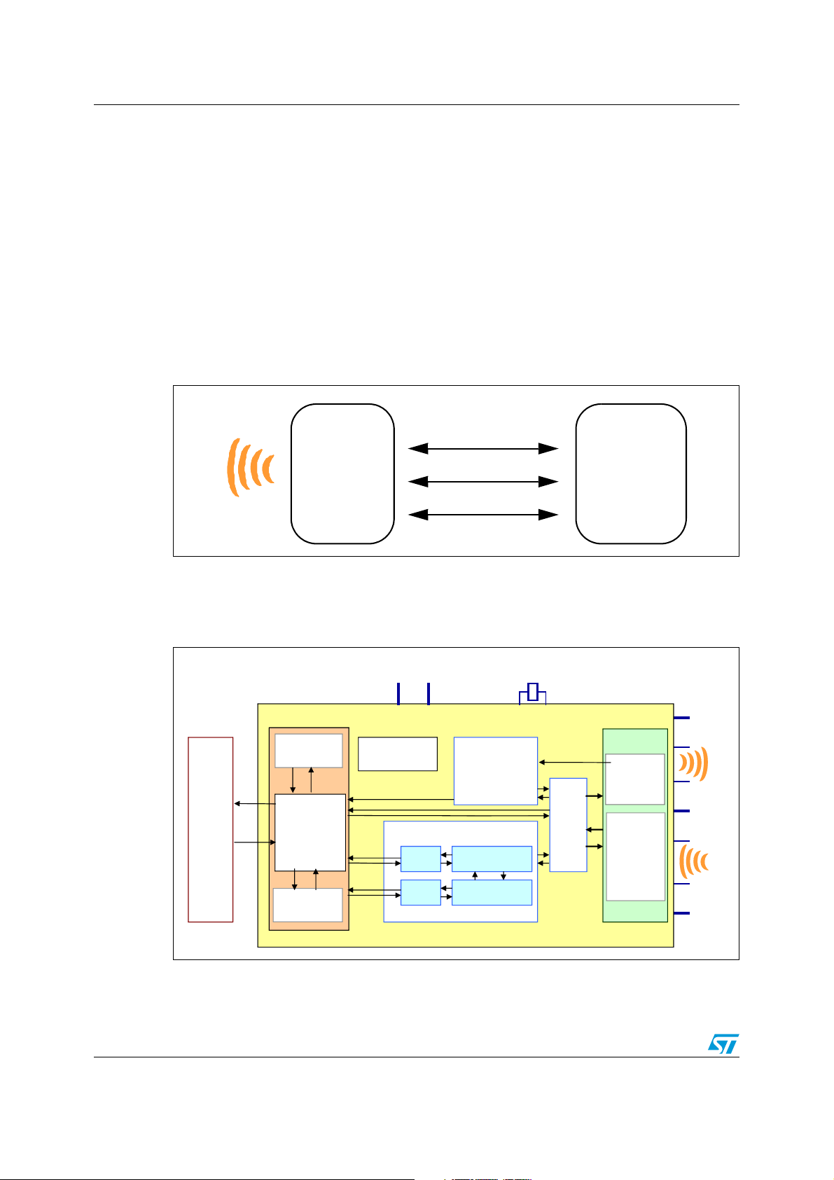
The CR95HF is an integrated transceiver IC for contactless applications.
The CR95HF manages frame coding and decoding in Reader mode for standard
applications such as near field communication (NFC), proximity and vicinity standards.
The CR95HF embeds an Analog Front End to provide the 13.56 MHz Air Interface.
The CR95HF supports ISO/IEC 14443 Type A and B, ISO/IEC 15693 (single or double
subcarrier) and ISO/IEC 18092 protocols.
The CR95HF also supports the detection, reading and writing of NFC Forum Type 1, 2, 3
and 4 tags.
Figure 1. CR95HF application overview
1.1 Block diagram
Figure 2. CR95HF block diagram
4/63 Doc ID 018669 Rev 8
Page 5

CR95HF Description
1.2 List of terms
Table 1. List of terms
Term Meaning
DAC Digital analog converter
GND Ground
HFO High frequency oscillator
LFO Low frequency oscillator
MCU Microcontroller unit
NFC Near Field Communication
RFID Radio Frequency Identification
RFU Reserved for future use
SPI Serial peripheral interface
t
L
t
REF
UART Universal asynchronous receiver-transmitter
WFE Wait For Event
Low frequency period
Reference time
Doc ID 018669 Rev 8 5/63
Page 6
Pin and signal descriptions CR95HF
1
17
25
9
VPS_TX
GND_TX
XOUT
XIN
NC
NC
NC
GND
ST_R1
SSI_1
SPI_MISO
SPI_SS
UART_RX / IRQ_IN
VPS
TX1
TX2
NC
NC
RX1
Shaded area represents the dissipation pad.
(Must be connected to ground.)
RX2
NC
GND_RX
NC
NC
NC
SSI_0
SPI_SCK
SPI_MOSI
NC
NC
ST_R0
UART_TX / IRQ_OUT
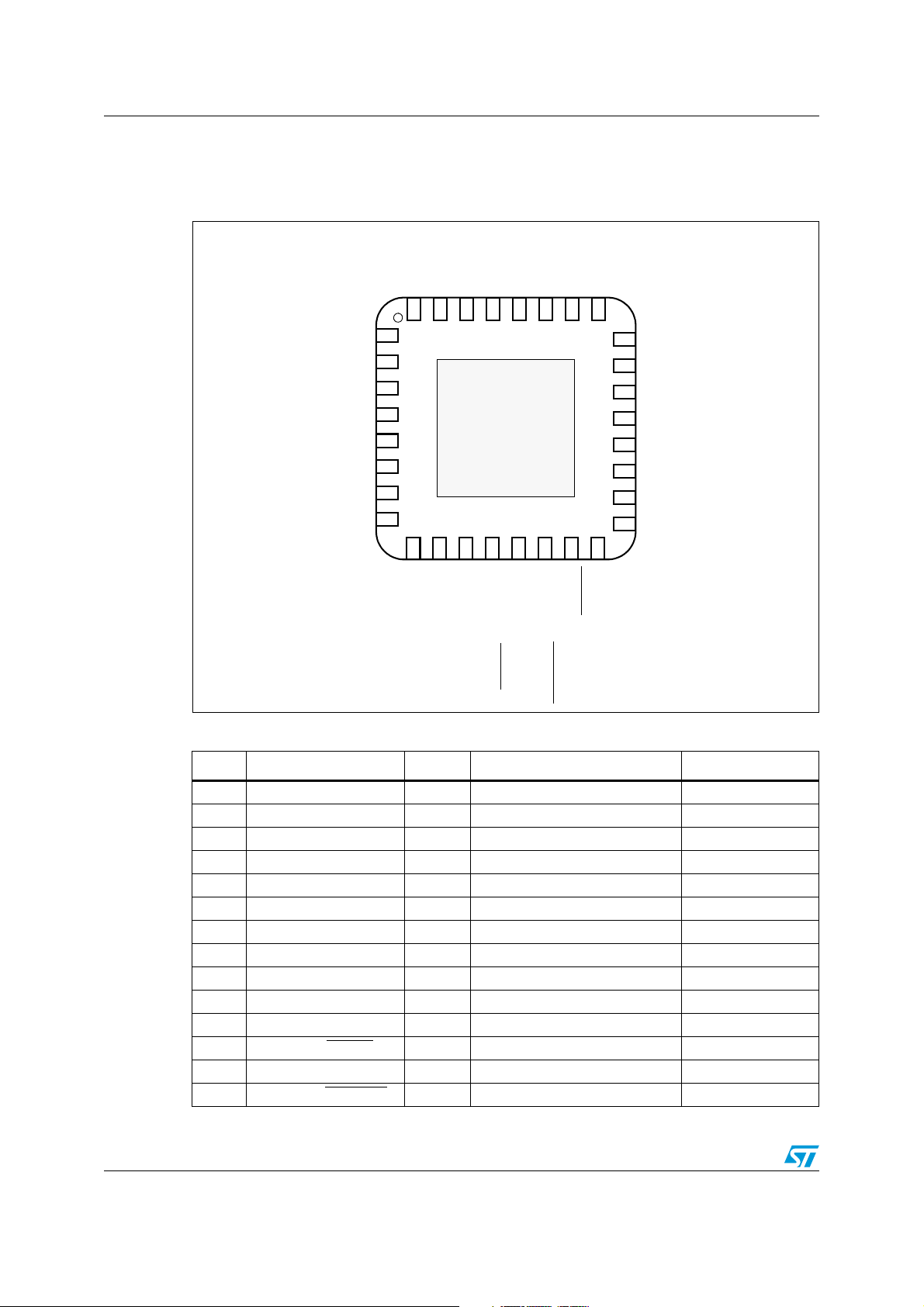
2 Pin and signal descriptions
Figure 3. Pinout description
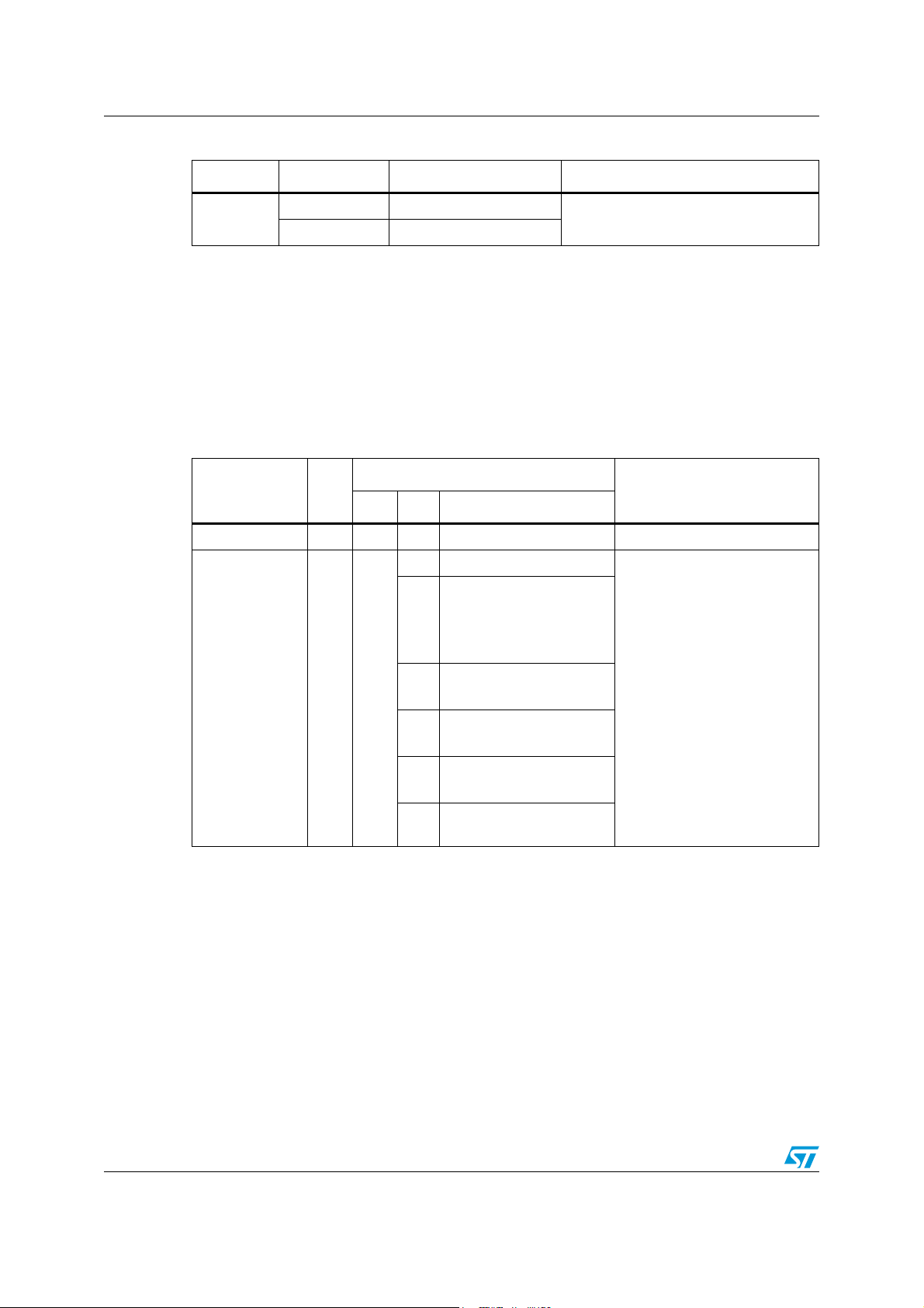
Table 2. Pin descriptions
Pin Pin name Type
(1)
1 TX1 O Driver output 1
2 TX2 O Driver output 2
3 NC Not connected
4 NC Not connected
5 RX1 I Receiver input 2
6 RX2 I Receiver input 1
6/63 Doc ID 018669 Rev 8
7 NC Not connected
8 GND_RX P Ground (analog)
9 ST_R0 O ST Reserved
10 NC Not connected
11 NC Not connected
12 UART_RX / IRQ_IN
13 VPS P Main power supply
14 UART_TX / IRQ_OUT
(3)
I
UART receive pin
O UART transmit pin Interrupt output
Main function Alternate function
(2)
(4)
Interrupt input
Page 7

CR95HF Pin and signal descriptions
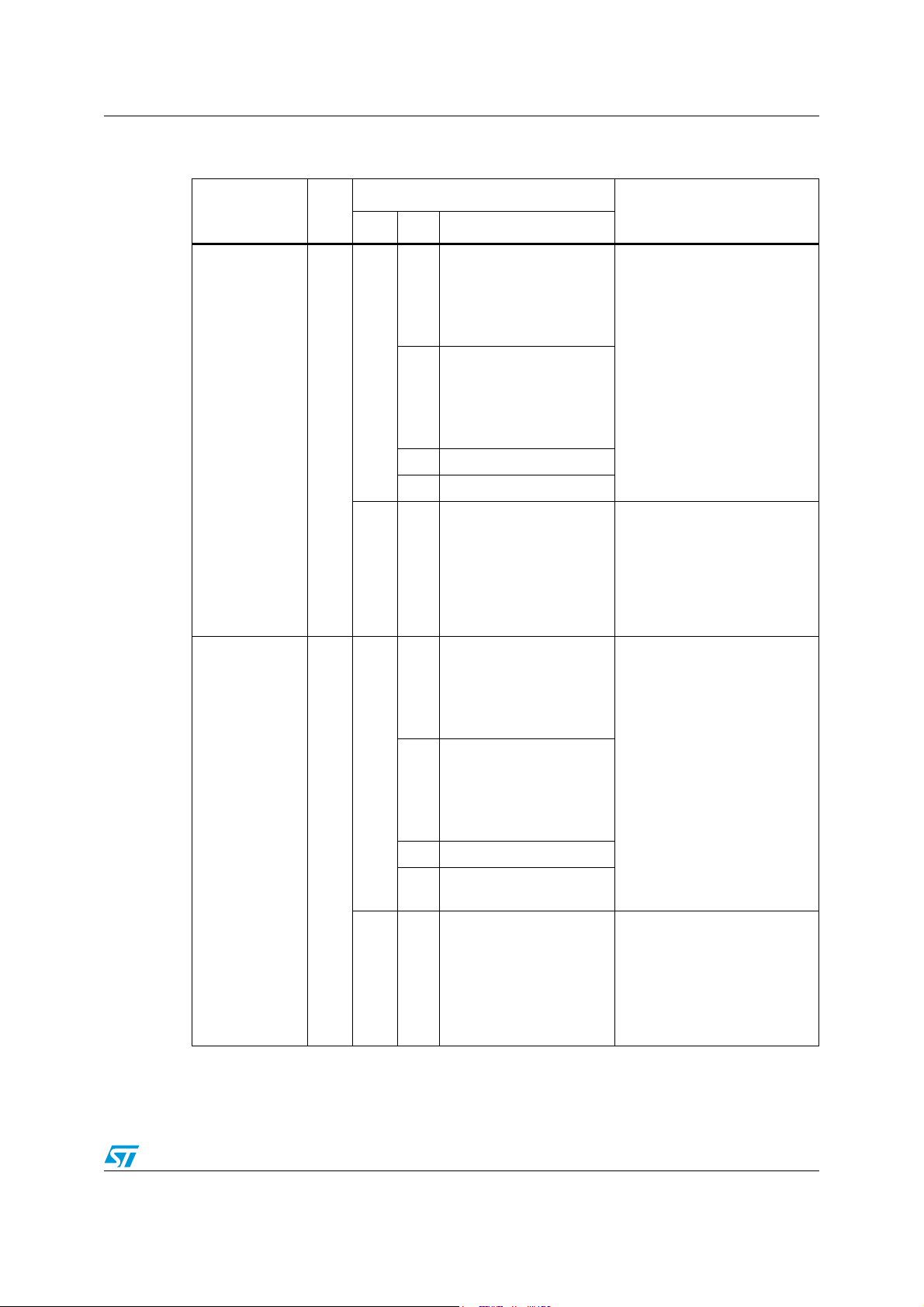
Table 2. Pin descriptions (continued)
Pin Pin name Type
15 SPI_SS
16 SPI_MISO O SPI Data, Slave Output
17 SPI_MOSI I SPI Data, Slave Input
18 SPI_SCK I
19 SSI_0 I
20 SSI_1 I
21 ST_R1 I
22 GND P Ground (digital)
23 NC Not connected
24 NC Not connected
25 NC Not connected
26 NC Not connected
27 NC Not connected
28 NC Not connected
29 XIN Crystal oscillator input
30 XOUT Crystal oscillator output
31 GND_TX P Ground (RF drivers)
32 VPS_TX P Power supply (RF drivers)
1. I: Input, O: Output, and P: Power
2. Must add a capacitor to ground (~1 nF).
3. Pad internally connected to a Very Weak Pull-up to VPS.
4. We recommend connecting this pin to the V
5. Pad internally connected to a Weak Pull-up to VPS.
6. Must not be left floating.
7. Pad internally connected to a Weak Pull-down to GND.
8. Pad input in High Impedance. Must be connected to VPS.
(1)
(5)
I
SPI Slave Select (active low)
(7)
SPI serial clock
Main function Alternate function
Select serial communication
interface
Select serial communication
interface
(8)
ST Reserved
pin using a 3.3 kOhm pull-up resistor.
PS
(6)
Doc ID 018669 Rev 8 7/63
Page 8

Power management and operating modes CR95HF
3 Power management and operating modes
3.1 Operating modes
The CR95HF has 2 operating modes: Wait for Event (WFE) and Active. In Active mode, the
CR95HF communicates actively with a tag or an external host (an MCU, for example). WFE
mode includes four low consumption states: Power-up, Hibernate, Sleep and Tag Detector.
The CR95HF can switch from one mode to another.
Table 3. CR95HF operating modes and states
Mode State Description
This mode is accessible directly after POR.
Wait For
Event
(WFE)
Active
Power-up
Hibernate
Sleep
Tag De te cto r
Ready
Reader
Low level on IRQ_IN
source. LFO (low-frequency oscillator) is running in this state.
Lowest power consumption state. The CR95HF has to be woken-up
in order to communicate. Low level on IRQ_IN pin (longer than 10 µs)
is the only wakeup source.
Low power consumption state. Wakeup source is configurable:
–Timer
–IRQ_IN
– SPI_SS pin
LFO (low-frequency oscillator) is running in this state.
Low power consumption state with tag detection. Wakeup source is
configurable:
–Timer
–IRQ_IN
– SPI_SS
– Tag detector
LFO (low-frequency oscillator) is running in this state.
In this mode, the RF is OFF and the CR95HF waits for a command
(P
interface (UART or SPI).
The CR95HF can communicate with a tag using the selected
protocol or with an external host using the selected serial interface
(UART or SPI).
pin
pin
pin
ROTOCOLSELECT, ...) from the external host via the selected serial
pin (longer than 10 µs) is the only wakeup
Hibernate, Sleep and Tag Detector states can only be activated by a command from the
external host. As soon as any of these three states are activated, the CR95HF can no
longer communicate with the external host. It can only be woken up.
The behavior of the CR95HF in 'Tag Detector' state is defined by the Idle command.
8/63 Doc ID 018669 Rev 8
Page 9
CR95HF Power management and operating modes
Supply off
Power-up
POR
Ready
Reader
Tag Detector
(& Calibration )
Sleep
IRQ_IN
Protocol Select
POR sequence Wake-up event
Hibernate
TimeOut
Tag Detection
Idle command
IRQ_IN
Activ e
WFE
IRQ_IN
Protocol Select
Serial I/F
selection
SPI
Reset
Figure 4. CR95HF initialization and operating state change
3.2 Startup sequence
After the power supply is established at power-on, the CR95HF waits for a low pulse on the
pin IRQ_IN
entering Ready state after a delay (t
Figure 5. Power-up sequence
1. Note for pin SSI0: - - - SPI selected, –––– UART selected
2. Pin IRQ_IN
Note: When CR95HF leaves WFE mode (from Power-up, Hibernate, Sleep or Tag Detector)
following an |RQ_IN
character.
(t1) before automatically selecting the external interface (SPI or UART) and
).
3
T
603
33)?
T
&IRSTVALID
T
COMMAND
-36
33)?
)21?).
low level < 0.2 VPS_Main.
/RX low level pulse, this pulse is NOT interpreted as the UART start bit
T
T
Doc ID 018669 Rev 8 9/63
Page 10
Power management and operating modes CR95HF
Figure 5 shows the power-up sequence for a CR95HF device; where,
● t
is the initial wake-up delay 100 µs (minimum)
0
● t
is the minimum interrupt width 10 µs (minimum)
1
● t
is the delay for the serial interface selection 250 ns (typical)
2
● t
is the HFO setup time (t
3
● t
is the VPS ramp-up time 10 ms (maximum by design
4
SU(HFO)
) 10 ms (maximum)
validation)
Note: The Serial Interface is selected after the following falling edge of pin IRQ_IN
from POR or Hibernate state.
Ta bl e 4 lists the signal configuration used to select the serial communication interface.
Table 4. Select serial communication interface selection table
Pin UART SPI
SSI_0 0 1
SSI_1 0 0
when leaving
10/63 Doc ID 018669 Rev 8
Page 11
CR95HF Communication protocols
Sending commands to the CR95HF
Receiving data from the CR95HF
CMD LEN DATA DATA
Several data bytes
Resp Code LEN DATA DATA
Several data bytes
Ai18122a
CR95HF
Internal
Clock
RX
TX
0123 4567
10101010
1 1
(Stop)
(Echo 0x55)
Host to CR95HF
RX
TX
CR95HF to Host
0
(Start)
10101010
1 1
(Stop)
(Echo 0x55)
0
(Start)
4 Communication protocols
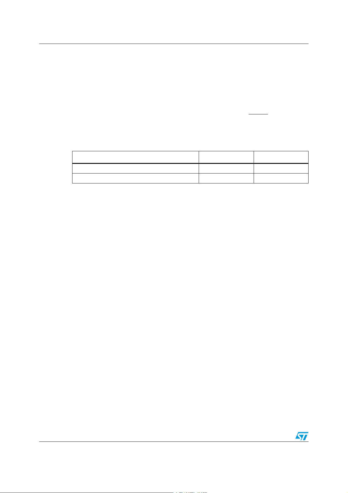
4.1 Universal asynchronous receiver/transmitter (UART)
The host sends commands to the CR95HF and waits for replies. Polling for readiness is not
necessary. The default baud rate is 57600 baud. The maximum allowed baud rate is
2 Mbps.
Figure 6. UART communication
When sending commands, no data must be sent if the LEN field is zero.
When receiving data from the CR95HF, no data will be received if the LEN field is zero.
The formats of send and receive packets are identical.
If an E
CHO command is sent, only one byte (0x55) is sent by the host.
Figure 7 shows an example of an E
Figure 7. ECHO command and response example
CHO command.
Caution: UART communication is LSB first. Stop bit duration is two Elementary Time Units
(ETUs).
Note: 1 When CR95HF leaves WFE mode (from Power-up, Hibernate, Sleep or Tag Detector)
following an |RQ_IN
character.
2 If the user loses UART synchronization, it can be recovered by sending an E
until a valid E
CR95HF will reply with an error code meaning its input buffer is full. The user can now
restart a UART exchange.
/RX low level pulse, this pulse is NOT interpreted as the UART start bit
CHO command
CHO reply is received. Otherwise, after a maximum of 255 ECHO commands,
Doc ID 018669 Rev 8 11/63
Page 12
Communication protocols CR95HF
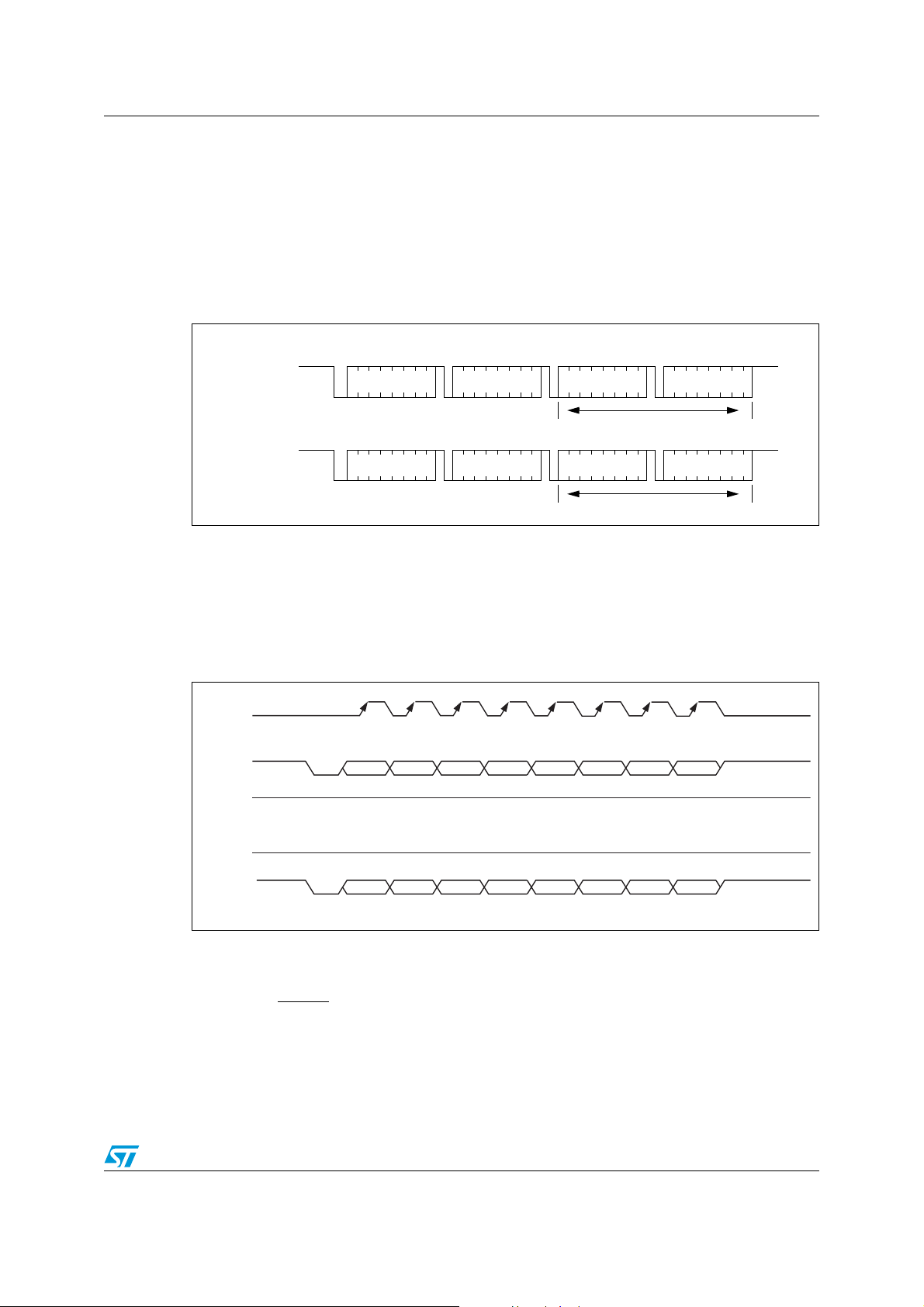
MOSI
0 0 0 0 0 0 0 0 CMD LEN DATA DATA
Control Byte
MISO
X X X X X X X X X X X X X X X X X X X X X X X X X X X X X X X X X X X X X X X X
Several data bytes
MOSI
0 0 0 0 0 0 1 1 X X X X X X 1 1 X X X X X X 1 1 X X X X X X 1 1
Control Byte
MISO
X X X X X X X X
Flag Flag
Flags are polled until data is ready (Bit 3 is set when data is ready)
0 0 0 0 0 X X X 0 0 0 0 0 X X X 0 0 0 0 1 X X X
4.2 Serial peripheral interface (SPI)
4.2.1 Polling mode
In order to send commands and receive replies, the application software has to perform 3
steps.
1. Send the command to the CR95HF.
2. Poll the CR95HF until it is ready to transmit the response.
3. Read the response.
The application software should never read data from the CR95HF without being sure that
the CR95HF is ready to send the response.
The maximum allowed SPI communication speed is f
SCK
.
A Control byte is used to specify a communication type and direction:
● 0x00: Send command to the CR95HF
● 0x03: Poll the CR95HF
● 0x02: Read data from the CR95HF
● 0x01: Reset the CR95HF
The SPI_SS
line is used to select a device on the common SPI bus. The SPI_SS pin is
active low.
When the SPI_SS
line is inactive, all data sent by the Master device is ignored and the
MISO line remains in High Impedance state.
Figure 8. Sending command to CR95HF
Figure 9. Polling the CR95HF until it is ready
Table 5. Interpretation of flags
Bit Meaning (Application point of view)
[7:4] Not significant
3 Data can be read from the CR95HF when set.
2 Data can be sent to the CR95HF when set.
[1:0] Not significant
12/63 Doc ID 018669 Rev 8
Page 13
CR95HF Communication protocols
MOSI
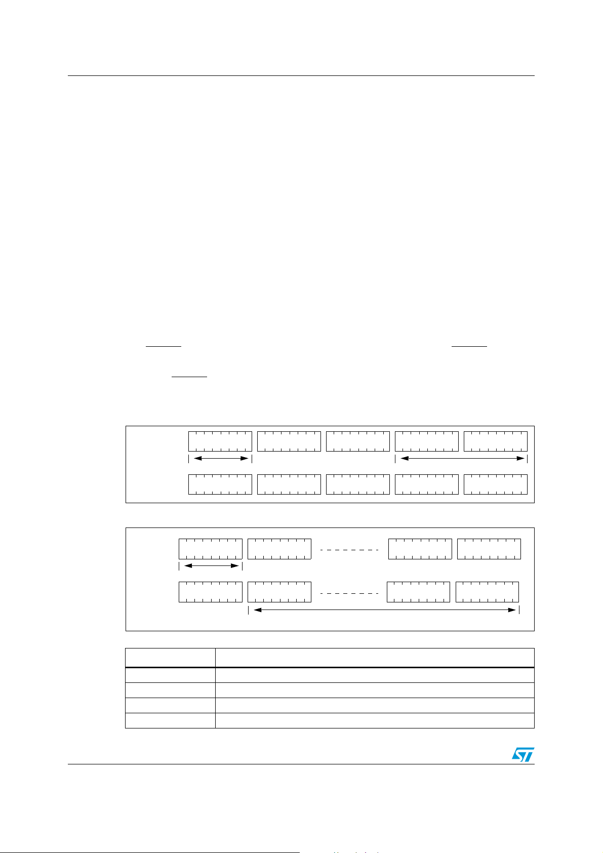
0 0 0 0 0 0 1 0 X X X X X X X X X X X X X X X X X X X X X X X X X X X X X X X X
Control Byte
MISO
X X X X X X X X Resp Code LEN DATA DATA
Several data bytes
MOSI
0 0 0 0 0 0 0 1
Control Byte 01
MISO
X X X X X X X X
Figure 10. Reading data from CR95HF
Data must be sampled at the rising edge of the SCK signal.
‘Sending’, ‘Polling’ and ‘Reading’ commands must be separated by a high level of the
SPI_SS
asserts the SPI_SS
line. For example, when the application needs to wait for data from the CR95HF, it
line low and issues a ‘Polling’ command. Keeping the SPI_SS line low,
the Host can read the Flags Waiting bit which indicates that the CR95HF can be read. Then,
the application has to assert the SPI_SS
asserts the SPI_SS
line low and issues a ‘Reading’ command to read data. When all data is
read, the application asserts the SPI_SS
line high to finish the polling command. The Host
line high.
The application is not obliged to keep reading Flags using the Polling command until the
CR95HF is ready in one command. It can issue as many 'Polling' commands as necessary.
For example, the application asserts SPI_SS
Flags. If the CR95HF is not ready, the application can assert SPI_SS
low, issues 'Polling' commands and reads
high and continue its
algorithm (measuring temperature, communication with something else). Then, the
application can assert SPI_SS
low again and again issue 'Polling' commands, and so on, as
many times as necessary, until the CR95HF is ready.
Note that at the beginning of communication, the application does not need to check flags to
start transmission. The CR95HF is assumed to be ready to receive a command from the
application.
Figure 11. Reset the CR95HF
To reset the CR95HF using the SPI, the application sends the SPI Reset command (Control
Byte 01, see Figure 11) which starts the internal controller reset process and puts the
CR95HF into Power-up state. The CR95HF will wake up when pin IRQ_IN
CR95HF reset process only starts when the SPI_SS
Caution: SPI communication is MSB first.
4.2.2 Interrupt mode
When the CR95HF is configure to use the SPI serial interface, pin IRQ_OUT is used to give
additional information to user. When the CR95HF is ready to send back a reply, it sends an
Interrupt Request by setting a low level on pin IRQ_OUT
reads the data.
goes low. The
pin returns to high level.
, which remains low until the host
The application can use the Interrupt mode to skip the polling stage.
Caution: SPI communication is MSB first.
Doc ID 018669 Rev 8 13/63
Page 14

Commands CR95HF
5 Commands
5.1 Command format
● The frame from the Host to the CR95HF has the following format:
<CMD><Len><Data>
● The frame from the CR95HF to Host has the following format:
<RespCode><Len><Data>
These two formats are available either in both UART and SPI modes.
Fields <Cmd>, <RespCode> and <Len> are always 1 byte long. <Data> can be from 0 to
255 bytes.
Note: The E
CHO command is an exception as it has only one byte (0x55).
The following symbols correspond to:
>>> Frame sent by the Host to CR95HF
<<< Frame sent by the CR95HF to the Host
5.2 List of commands
Ta bl e 6 summarizes the available commands.
Table 6. List of CR95HF commands
Code Command Description
0x01 IDN Requests short information about the CR95HF and its revision.
0x02 P
0x04 SENDRECV
0x07 I
0x08 R
0x09 W
ROTOCOLSELECT
DLE
DREG
RREG
Selects the RF communication protocol and specifies certain
protocol-related parameters.
Sends data using the previously selected protocol and receives the
tag response.
Switches the CR95HF into a low consumption Wait for Event (WFE)
mode (Power-up, Hibernate, Sleep or Tag detection), specifies the
authorized wake-up sources and waits for an event to exit to Ready
state.
Reads Wake-up event register or the Analog Register Configuration
(ARC_B) register.
Writes Analog Register Configuration (ARC_B) register or writes
index of ARC_B register address.
Writes the Timer Window (TimerW) value dedicated to ISO/IEC
14443 Type A tags.
Writes the AutoDetect Filter enable register dedicated to ISO/IEC
18092 tags.
0x0A B
0x55 E
14/63 Doc ID 018669 Rev 8
AUDRATE Sets the UART baud rate.
CHO CR95HF returns an ECHO response (0x55).
Other codes ST Reserved
Page 15

CR95HF Commands
5.3 IDN command (0x01) description
The IDN command (0x01) gives brief information about the CR95HF and its revision.
Table 7. IDN command description
Direction Data Comments Example
Host to
CR95HF
CR95HF to
Host
It takes approximately 6 ms to calculate the CRC for the entire ROM. The application must
allow sufficient time for waiting for a response for this command.
0x01 Command code
0x00 Length of data
0x00 Result code <<<0x000F4E4643204653324A41535
<Len> Length of data
<Device ID> Data in ASCII format
<ROM CRC>
CRC calculated for ROM
content
>>>0x0100
4320075D2
In this example,
<<<0x4E4643204653324A415354320
0: ‘NFC FS2JAST2’, #2 (Last Character
of NFC FS2JAST2 means ROM code
revision 2.)
0x75D2: CRC of ROM (real CRC may
differ from this example)
5.4 Protocol Select command (0x02) description
This command selects the RF communication protocol and prepares the CR95HF for
communication with a contactless tag.
Table 8. PROTOCOLSELECT command description
Direction Data Comments Example
0x02 Command code
<Len> Length of data
Protocol codes
00: Field OFF
See Table 9: List of <Parameters>
values for the ProtocolSelect command
for different protocols on page 16 for a
detailed example.
<<<0x0000
Protocol is successfully selected
<<<0x8200
Invalid command length
Host to
CR95HF
CR95HF to
Host
CR95HF to
Host
01: ISO/IEC 15693
<Protocol>
<Parameters>
0x00 Result code
0x00 Length of data
0x82 Error code
0x00 Length of data
02: ISO/IEC 14443-A
03: ISO/IEC 14443-B
04: ISO/IEC 18092 /NFC
Forum Tag Type 3
Each protocol has a
different set of
parameters. See Tab l e 9 .
Doc ID 018669 Rev 8 15/63
Page 16
Commands CR95HF
Table 8. PROTOCOLSELECT command description (continued)
Direction Data Comments Example
CR95HF to
Host
0x83 Error code
0x00 Length of data
<<<0x8300
Invalid protocol
Note that there is no ‘Field ON’ command. When the application selects an RF
communication protocol, the field automatically switches ON.
When the application selects a protocol, the CR95HF performs all necessary settings: it will
choose the appropriate reception and transmission chains, switch ON or OFF the RF field
and connect the antenna accordingly.
Different protocols have different sets of parameters. Values for the <Parameters> field
are listed in Ta bl e 9 .
Table 9. List of <Parameters> values for the PROTOCOLSELECT command for
different protocols
Parameters
Protocol Code
Byte Bit Function
Field OFF 0x00 07:0RFU >>>0x02020000
7:6 RFU
00: 26 Kbps (H)
01: 52 Kbps
5:4
10: 6 Kbps (L)
11: RFU
0: Respect 312-µs delay
ISO/IEC 15693 0x01 0
3
1: Wait for SOF
0: 100% modulation (100)
2
1: 10% modulation (10)
(1)
Examples of commands
H 100 S: >>>0x02 02 01 01
H 100 D: >>>0x02 02 01 03
H 10 S: >>>0x02 02 01 05
H 10 D: >>>0x02 02 01 07
L 100 S: >>>0x02 02 01 21
L 100 D: >>>0x02 02 01 23
L 10 S: >>>0x02 02 01 25
L 10 D: >>>0x02 02 01 27
0: Single subcarrier (S)
1
1: Dual subcarrier (D)
Append CRC if set to ‘1’.
0
(1)
16/63 Doc ID 018669 Rev 8
In these examples, the CRC is
automatically appended.
Page 17
CR95HF Commands
Table 9. List of <Parameters> values for the PROTOCOLSELECT command for
different protocols (continued)
Parameters
Protocol Code
Byte Bit Function
Examples of commands
ISO/IEC 14443
Ty p e A
NFC Forum Tag
Ty p e 1
(Topaz)
NFC Forum Tag
Ty p e 2
NFC Forum Tag
Type 4A
ISO/IEC 14443
Ty p e B
NFC Forum Tag
Type 4B
0x02
0x03
0
1, 2
0
Transmission data rate
00: 106 Kbps
7:6
01: 212 Kbps
10: RFU
11: RFU
Reception data rate
00: 106 Kbps
5:4
01: 212 Kbps
10: RFU
11: RFU
3RFU
2:0 RFU
AFDT (Optional) 2 bytes
0xPP 0xMM
Set the maximum CR95HF
listening time so that it fits
the maximum ISO FWT:
0xPP ≤ 0x0E,
0x01 ≤ 0xMM ≤ 0xFE
Transmission data rate
00: 106 Kbps
7:6
01: RFU
10: RFU
11: RFU
Reception data rate
00: 106 Kbps
5:4
01: RFU
10: RFU
11: RFU
3:1 RFU
Append CRC if set to ‘1’.
0
(1)
(2)
(2)
>>>0x02020200: ISO/IEC
14443 Type A tag, 106 Kbps
transmission and reception
rates, Time interval 86/90
Note that REQA, WUPA,
Select20 and Select70
commands use a fixed interval
of 86/90 µs between a request
and its reply. Other commands
use a variable interval with fixed
granularity.
Refer to the ISO/IEC 14443
standard for more details.
Frame Waiting Time (FWT) =
PP
) *(MM+1) * 4096/13.56 µs
(2
If AFDT is not specified,
the default FWT is ~ 86 µs
>>>0x02020301:
ISO/IEC 14443 Type B tag with
CRC appended
AFDT (Optional) 2 bytes
1, 2
0xPP 0xMM
Set the maximum CR95HF
listening time so that it fits
the maximum ISO FWT:
0xPP ≤ 0x0E,
Frame Waiting Time (FWT) =
PP
) *(MM+1) * 4096/13.56 µs
(2
If AFDT is not specified,
the default FWT is ~ 4.8 ms
0x01 ≤ 0xMM ≤ 0xFE
Doc ID 018669 Rev 8 17/63
(3)
Page 18

Commands CR95HF
Table 9. List of <Parameters> values for the PROTOCOLSELECT command for
different protocols (continued)
Parameters
Protocol Code
ISO/IEC 18092
NFC Forum Tag
Ty p e 3
0x04
Byte Bit Function
Transmission data rate
00: RFU
7:6
01: 212 Kbps
10: 424 Kbps
11: RFU
Reception data rate
0
5:4
00: RFU
01: 212 Kbps
10: 424 Kbps
11: RFU
3:1 RFU
Append CRC if set to ‘1’.
0
(1)
7:5 RFU
Disregard slot counter
4
0: Respect slot counter
1: Search for the reply
1
Slot counter
0: 1 slot
3:0
1: 2 slots
…
F: 16 slots
Examples of commands
>>>0x02020451:
ISO/IEC18092 tag, 212 Kbps
transmission and reception
rates with CRC appended.
Parameter ‘Slot counter’ is not
mandatory. If it is not present, it
is assumed that SlotCounter =
0x00 (1 slot)
For device detection
commands, byte 1 bit 4 must be
set to ‘0’. In this case, the FWT
is 2.4 ms for the 1st slot and
1.2 ms more for each following
slot, if slot counter is specified.
If slot counter = 0x10, the
CR95HF does not respect reply
timings, but polls incoming data
and searches a valid response
during ~8.4 ms.
AFDT (Optional) 2 bytes
0xPP 0xMM
Set the maximum CR95HF
2,3
listening time so that it fits
the maximum ISO FWT:
0xPP ≤ 0x0E,
0x01 ≤ 0xMM ≤ 0xFE
1. It is recommended to set this bit to ‘1’.
2. Not characterized.
3. Max TR1 (Synchronization Time as defined in ISO/IEC 14443-2, Type B) supported by the CR95HF is 170
µs. This value will be increased to 302 µs in the next CR95HF revision.
18/63 Doc ID 018669 Rev 8
Frame Waiting Time (FWT) =
PP
) *(MM+1) * 4096/13.56 µs
(2
If AFDT is not specified,
the default FWT is ~ 302 µs
Page 19
CR95HF Commands
5.5 Send Receive (SendRecv) command (0x04) description
This command sends data to a contactless tag and receives its reply.
Before sending this command, the Host must first send the P
ROTOCOLSELECT command to
select an RF communication protocol.
If the tag response was received and decoded correctly, the <Data> field can contain
additional information which is protocol-specific. This is explained in Tab l e 1 1.
Table 10. SENDRECV command description
Direction Data Comments Example
0x04 Command code
Host to
CR95HF
CR95HF to
Host
CR95HF to
Host
CR95HF to
Host
CR95HF to
Host
<Len> Length of data
<Data> Data to be sent
0x80 Result code
<Len> Length of data
Data received.
<Data>
0x90 Result code
0x04 Vali d b its
ACK or NAK
0x86 Error code
0x00 Length of data
0x87 Error code
0x00 Length of data
Interpretation depends on
protocol
ISO 14443-A
ACK or NAK detection
See Ta b le 1 1 and Ta b le 1 2 for detailed
examples.
<<<0x800F5077FE01B30000000000
71718EBA00
The tag response is decoded. This is an
example of an ISO/IEC 14443 ATQB
response (Answer to Request Type B)
<<<0x900400
Exception for 4-bit frames. This function
is limited.
ACK/NAK always returns ‘0’.
<<<0x8600 Communication error
<<<0x8700 Frame wait time out or no
tag
(1)
CR95HF to
Host
CR95HF to
Host
CR95HF to
Host
CR95HF to
Host
CR95HF to
Host
CR95HF to
Host
0x88 Error code
0x00 Length of data
0x89 Error code
0x00 Length of data
0x8A Error code
0x00 Length of data
0x8B Error code
0x00 Length of data
0x8C Error code <<<0x8C00 Invalid length. Used in NFC
0x00 Length of data
0x8D Error code
0x00 Length of data
Doc ID 018669 Rev 8 19/63
<<<0x8800 Invalid SOF
<<<0x8900 Receive buffer overflow
(too many bytes received)
<<<0x8A00 Framing error (start bit = 0,
stop bit = 1)
<<<0x8B00 EGT time out (for ISO/IEC
14443-B)
Forum Tag Type 3, when field Length <
3
<<<0x8D00 CRC error (Used in NFC
Forum Tag Type 3 protocol)
Page 20

Commands CR95HF
Table 10. SENDRECV command description (continued)
Direction Data Comments Example
CR95HF to
Host
1. ACK/NAK value will be correctly reported in next CR95HF revision.
0x8E Error code
0x00 Length of data
<<<0x8E00 Reception lost without EOF
received
Ta bl e 1 1 gives examples of communication between the CR95HF and a contactless tag.
The CR95HF receives a SendRecv command (>>> 0x04...) from the host and returns its
response to the host (<<< 0x80...). Ta bl e 1 1 provides more details on the CR95HF
response format.
Table 11. List of <Data> Send values for the SENDRECV command for different
protocols
Protocol Explanation Command example Comments
Send example 04 03 022000 Example of an Inventory command
Command code
Length of entire data field
ISO/IEC
15693
Data
using different protocol configuration:
Uplink: 100% ASK, 1/4 coding
Downlink: High data rate, Single sub-
carrier
>>> 0x0403260100 (Inventory - 1 slot)
<<< 0x800D0000CDE0406CD62902
E0057900
If length of data is ‘0’, only the EOF will
be sent. This can be used for an anticollision procedure.
20/63 Doc ID 018669 Rev 8
Page 21

CR95HF Commands
Table 11. List of <Data> Send values for the SENDRECV command for different
protocols (continued)
Protocol Explanation Command example Comments
ISO/IEC
14443
Ty p e A
NFC
Forum Tag
Type 4A
NFC
Forum Tag
Type 1
(Topaz)
NFC
Forum Tag
Ty p e 2
Send example 04 07
Command code
Length of entire data field
Data
Transmission flags:
7: Topaz send format. Use EOF instead of
parity bit and use SOF at beginning of each
byte. Pause between bytes and assume 1st
byte is 7 bits.
6: SplitFrame
5: Append CRC
4: Do not decode parity bit for proprietary
framing
[3:0]: 8 – number of significant bits in last byte
9370800
F8C8E
28
Example of an NFC Forum Type 2
request sequence:
>>>0x04022607 (REQA)
<<<0x800544002800 (ATQA)
>>>0x0403932008 (Anti-collision CL1)
<<<0x80088804A8D5F1280000 (UID
CL1)...
Example of an NFC Forum Type 1
(Topaz) request sequence:
>>>0x04022607 (REQA)
<<<0x8005000C280000 (ATQ0 ATQ1)
>>>0x040878000000000000A8 (RID)
<<<0x800B11486E567A003E450800
00 (Header0 Header1 UID0 UID 1 UID2
UID3 CRC0 CRC1Signifcant bits
indexColbyte IndexColbit)
Application SW must specify how many
bits to send in the last byte. If flag
SplitFrame is set, CR95HF will expect
8 – <significant bit count> bits in the 1
byte during reception. Otherwise it
expects 8 bits.
st
ISO/IEC
14443
Ty p e B
NFC
Forum Tag
Type 4B
ISO/IEC
18092
NFC
Forum Tag
Type 3
Send example 04 03 050000
Command code
Length of entire data field
Data
Send example 04 05 00FFFF0000
Command code
Length of entire data field
Data
This command is useful for anti-collision.
Example of an NFC Forum Type 4B
request sequence:
>>>0x0403050000 (REQB)
<<<0x800F5077FE01B30000000000
71718EBA00 (ATQB)
Example of an ISO/IEC 18092 / NFC
Forum Type 3 request sequence:
>>>0x040500FFFF0000 (REQC)
<<<0x801201010102148E0DB41310
0B4B428485D0FF00 (ATQC)
Doc ID 018669 Rev 8 21/63
Page 22

Commands CR95HF
Table 12. List of <Data> Response values for the SENDRECV command for different
protocols
Protocol Explanation Response example Comments
ISO/IEC
15693
ISO/IEC
14443
Ty p e A
NFC
Forum
Tag Type
4A
NFC
Forum
Tag Type
1
(Topaz)
Response
example
80 08 0000000000 77CF 00
Result code
Length of entire data
field
Data received from tag
Original (received) value of CRC
[7:2]: RFU
1: CRC error if set
0: Collision is detected if set
Response
example
80 09 80B30B8DB500 00 00 00
Result code
Length of entire data
field
Data received from TAG
7: Collision is detected
6: RFU
5: CRC error
4: parity error
[3:0]: Shows how many significant bits are there
in the first byte
7:0: Index of the first byte where collision is detected
This is a response on Read
Single Block command for
ISO/IEC 15693 TAG. Actual
TAG response is
<<<0x000000000077CF,
other fields are added by the
CR95HF.
ISO/IEC 14443-A is bit
oriented protocol, so we can
receive non-integer amount
of bytes. Number of
significant bits in the 1
st
byte
is the same as indicated in
the command sent.
To calculate a position of a
collision, application has to
take index of byte first. Index
of bit indicates a position
inside this byte. Note that
both indexes start from 0 and
bit index can be 8, meaning
that collision affected parity.
NFC
Forum
Tag Type
[7:4]: RFU
[3:0]: Index of the first bit where collision is detected
2
Response
example
80 0F
5092036A8D0
00000000071713411 00
ISO/IEC
14443
Ty p e B
Result code
Length of entire data
field
NFC
Forum
Tag Type
4B
Data received from tag
Original (received) value of CRC
[7:2]: RFU
1: CRC error if set
0: RFU
22/63 Doc ID 018669 Rev 8
Note that collision
information is only valid when
bit ‘Collision is detected’ is
set.
Page 23

CR95HF Commands
Table 12. List of <Data> Response values for the SENDRECV command for different
protocols (continued)
Protocol Explanation Response example Comments
ISO/IEC
18092
NFC
Forum
Tag Type
3
Response
example
Result code
Length of entire data
field
Data received from tag
[7:2]: RFU
1: CRC error if set
0: RFU
80 12 01010105017B0...93FF 00
<<<0x801201010105017B
06941004014B024F4993F
F00
For more detailed examples of use with NFC Forum and ISO/IEC 15693 tags, refer to
Appendix D on page 51.
5.6 Idle command (0x07) description
This command switches the CR95HF into low consumption mode and defines the way to
return to Ready state.
The Result code contains the Wake-up flag register value indicating to the application the
wake-up event that caused the device to exit WFE mode.
Doc ID 018669 Rev 8 23/63
Page 24

Commands CR95HF
Table 13. Idle command description
Direction Data Comments Example
07 Command code
0E Length of data
Specifies authorized wake-
Host to
CR95HF
<WU Source>
EnterCtrlL
EnterCtrlH
WUCtrlL
WUCtrlH
LeaveCtrlL Settings to leave WFE
LeaveCtrlH
<WUPeriod>
<OscStart>
<DacStart>
<DacDataL>
<DacDataH>
<SwingsCnt>
<MaxSleep>
up sources and the LFO
frequency
Settings to enter WFE
mode
Settings to wake-up from
WFE mode
mode (Default value =
0x1800)
Period of time between two
tag detection bursts. Also
used to specify the duration
before Timeout.
Defines the Wait time for
HFO to stabilize:
<OscStart> * t
L
(Default value = 0x60)
Defines the Wait time for
DAC to stabilize:
<DacStart> * t
L
(Default value = 0x60)
Lower compare value for
tag detection
(1)
.
This value must be set to
0x00 during tag detection
calibration.
Higher compare value for
tag detection
(1)
.
This is a variable used
during tag detection
calibration.
Number of swings HF
during tag detection
(Default value = 0x3F)
Max. number of tag
detection trials before
Timeout
(1)
.
This value must be set to
0x01 during tag detection
calibration.
Also used to specify
duration before Timeout.
MaxSleep must be:
0x00 < MaxSleep < 0x1F
Example of switch from Active
mode to Hibernate state:
>>>0x07 0E 08 04 00 04 00
18 00 00 00 00 00 00 00 00
Example of switch from Active to
WFE mode (wake-up by low pulse
on IRQ_IN
pin):
>>>0x07 0E 08 01 00 38 00
18 00 00 60 00 00 00 00 00
Example of switch from Active to
WFE mode (wake-up by low pulse
on SPI_SS
pin):
>>>0x07 0E 10 01 00 38 00
18 00 00 60 00 00 00 00 00
Example of wake-up by Timeout (7
seconds):
Duration before Timeout = 256 * t
* (WU period + 2) * (MaxSleep + 1)
>>>0x07 0E 01 21 00 38 00
18 00 60 60 00 00 00 00 08
Example of switch from Active to
Tag Detector mode (wake-up by
tag detection or low pulse on
pin) (32 kHz, inactivity
IRQ_IN
duration = 272 ms, DAC oscillator
= 3 ms, Swing = 63 pulses of 13.56
MHz):
>>>0x07 0E 0A 21 00 79 01
18 00 20 60 60 64 74 3F 08
Example of a basic Idle command
used during the Tag Detection
Calibration process:
>>>0x07 0E 03 A1 00 F8 01
18 00 20 60 60 00 xx 3F 01
where xx is the DacDataH value.
L
24/63 Doc ID 018669 Rev 8
Page 25

CR95HF Commands
Table 13. Idle command description (continued)
Direction Data Comments Example
0x00 Result code
This response is sent only when
CR95HF exits WFE mode.
<<<0x000101 Wake-up by
Timeout
<<<0x000102 Wake-up by tag
detect
<<<0x000108 Wake-up by low
pulse on IRQ_IN
pin
CR95HF to
Host
0x01 Length of data
Data (Wake-up source)
0x01: Timeout
0x02: Tag detect
<Data>
0x08: Low pulse on
IRQ_IN
pin
0x10: Low pulse on
SPI_SS pin
CR95HF to
Host
1. An initial calibration is necessary to determine DacDataL and DacDataH values required for leaving Tag
Detector state. For more information, contact your ST sales office for the corresponding application note.
0x82 Error code
0x00 Length of data
<<<0x8200 Invalid command
length
5.6.1 Idle command parameters
The Idle command (Host to CR95HF) has the following structure (all values are
hexadecimal):
Table 14. Idle command structure
07 0E xx yy zz yy zz yy zz aa bb cc dd ee ff gg
Comma
nd code
Data
length
WU
source
Enter
Control
WU
Control
Leave
Control
WU
Period
Osc
Start
DAC
Start
DAC
Data
Swing
Count
Max
Sleep
Table 15. Summary of parameters
Parameter Description
Command code
Data length
This byte is the command code. ‘07’ represents the Idle command. This
command switches the device from Active mode to WFE mode.
This byte is the length of the command in bytes. Its value depends on the
following parameter values.
This byte defines the authorized wake-up sources in the Wake-up source
WU Source
register. Predefined values are:
0x01: Time out 0x02: Tag Detection
0x08: Low pulse on IRQ_IN
These two bytes (EnterCtrlL and EnterCtrlH) define the resources when
entering WFE mode.
Enter Control
0x0400: Hibernate
0x0100: Sleep (or 0x2100 if Timer source is enabled)
0xA200: Tag Detector Calibration
0x2100: Tag Detection
These two bytes (WuCtrlL and WuCtrlH) define the wake-up resources.
WU Control
0x0400: Hibernate 0x3800: Sleep
0xF801: Tag Detector Calibration 0x7901: Tag Detection
0x10: Low pulse on SPI_SS
Doc ID 018669 Rev 8 25/63
Page 26

Commands CR95HF
Table 15. Summary of parameters (continued)
Parameter Description
These two bytes (LeaveCtrlL and LeaveCtrlH) define the resources when
Leave Control
WU Period
Osc Start
DAC Start
DAC Data
returning to Ready state.
0x1800: Hibernate 0x1800: Sleep
0x1800: Tag Detector Calibration 0x1800: Tag Detection
This byte is the coefficient used to adjust the time allowed between two tag
detections. Also used to specify the duration before Timeout. (Typical
value: 0x20)
Duration before Timeout = 256 * tL * (WU period + 2) * (MaxSleep + 1)
This byte defines the delay for HFO stabilization. (Recommended value:
0x60)
Defines the Wait time for HFO to stabilize: <OscStart> * t
This byte defines the delay for DAC stabilization. (Recommended value:
0x60)
Defines the Wait time for DAC to stabilize: <DacStart> * t
These two bytes (DacDataL and DacDataH) define the lower and higher
comparator values, respectively. These values are determined by a
calibration process.
When using the demo board, these values should be set to approximately
0x64 and 0x74, respectively.
L
L
Swing Count
Max Sleep
This byte defines the number of HF swings allowed during Tag Detection.
(Recommended value: 0x3F)
This byte defines the maximum number of tag detection trials or the
coefficient to adjust the maximum inactivity duration before Timeout.
MaxSleep must be: 0x00 < MaxSleep < 0x1F
This value must be set to 0x01 during tag detection calibration.
Also used to specify duration before Timeout.
Duration before Timeout = 256 * t
(Typical value: 0x28)
* (WU period + 2) * (MaxSleep + 1)
L
5.6.2 Using LFO frequency setting to reduce power consumption
In WFE mode, the high frequency oscillator (HFO) is stopped and most processes being
executed are clocked by the low frequency oscillator (LFO). To minimize CR95HF power
consumption in WFE mode, the slower the LFO frequency, the lower the power
consumption.
Example 1: Setting a lower LFO frequency
The following equation defines a basic timing reference:
t
= 256*tL ms (where tL = 1/f
REF
t
= 8 ms (when bits [7:6] are set to “00”, or 32 kHz)
REF
t
= 64 ms (when bits [7:6] are set to “11”, or 4 kHz)
REF
LFO
)
26/63 Doc ID 018669 Rev 8
Page 27

CR95HF Commands
5.6.3 Optimizing wake-up conditions
Using the Wake-up source register, it is possible to cumulate sources for a wake-up event. It
is strongly recommended to always set an external event as a possible wake-up source.
To cumulate wake-up sources, simply set the corresponding bits in the Wake-up source
register. For example, to enable a wake-up when a tag is detected (bit 1 set to ‘1’) or on a
low pulse on pin IRQ_IN
(bit 3 set to ‘1’), set the register to 0x0A.
5.6.4 Using various techniques to return to Ready state
The Idle command and reply set offers several benefits to users by enabling various
methods to return the CR95HF to Ready state. Some methods are nearly automatic, such
as waiting for a timer overflow or a tag detection, but others consume more power compared
to the ones requesting a host action. A description of each method follows below.
Default setting: from POR to Ready state
After power-on, the CR95HF enters Power-up state.
To wake up the CR95HF and set it to Ready state, the user must send a low pulse on the
IRQ_IN
and enters Ready state and is able to accept commSands after a delay of approximately
6ms (t
pin. The CR95HF then automatically selects the external interface (SPI or UART)
).
3
From Ready state to Hibernate state and back to Ready state
In Hibernate state, most resources are switched off to achieve an ultra-low power
consumption.
The only way the CR95HF can wake-up from Hibernate state is by an external event (low
pulse on pin IRQ_IN
A basic Idle command is:
>>>0x07 0E 08 04 00 04 00 18 00 00 00 00 00 00 00 00
Note: The Wake-up flag value is NOT significant when returning to Ready state from Hibernate
state or after a POR.
).
From Ready state to Sleep state and back to Ready state
Wake-up by external event (low pulse on IRQ_IN or SPI_SS pin)
In Sleep or Power-up states, operating resources are limited in function of the selected
wake-up source to achieve a moderate power consumption level.
An Idle command example when wake-up source is pin IRQ_IN
>>>0x07 0E 08 01 00 38 00 18 00 00 60 00 00 00 00 00
A similar command can be implemented using pin SPI_SS
>>>0x07 0E 10 01 00 38 00 18 00 00 60 00 00 00 00 00
Wake-up by Timeout
:
as a wake-up source:
The LFO is required to use the timer. However, this increases the typical power consumption
by 80 µA. Several parameters can be modified to reduce power consumption as much as
possible.
Doc ID 018669 Rev 8 27/63
Page 28

Commands CR95HF
The Duration before Timeout is defined by parameters WU period and MaxSleep,
respectively 0x60 and 0x08 in the following example.
Duration before Timeout = 256 * t
L
Note: Note that: 0x00 < MaxSleep < 0x1F.
An Idle command example when wake-up source is timer (0x01) when f
power consumption is 25 µA)
>>>0x07 0E 01 21 00 38 00 18 00 60 60 00 00 00 00 08
An Idle command example when wake-up source is timer (0xC1) when f
power consumption is 20 µA):
>>>0x07 0E C1 21 00 38 00 18 00 60 60 00 00 00 00 08
The same command can be used mixing a timer and the IRQ_IN
source:
>>>0x07 0E C9 21 00 38 00 18 00 60 60 00 00 00 00 08
Wake-up by Tag Detection
In this mode, the typical consumption can greatly vary in function of parameter settings (WU
period without RF activity and Swing Count defining the RF burst duration). Using default
settings, consumption in the range of 100 µA can be achieved.
Tag Detector is a state where CR95HF is able to detect an RF event, a wake-up will occur
when a tag sufficiently modifies the antenna load and is detected by the CR95HF.
An Idle command example when wake-up source is Tag Detection (0x02):
>>>0x07 0E 02 21 00 79 01 18 00 20 60 60 64 74 3F 08
* (WU period + 2) * (MaxSleep + 1)
pin (0xC9) as a wake-up
= 32 kHz (mean
LFO
= 4 kHz (mean
LFO
The same command can be used mixing Tag Detection and the IRQ_IN
pin (0x0A) as a
wake-up source:
>>>0x07 0E 0A 21 00 79 01 18 00 20 60 60 64 74 3F 08
The tag detection sequence is defined by dedicated parameters:
● WU source (Byte 3) (Wake-up source register on page 46)
– The Timeout bit (bit 0) must be set to ‘1’ in order to manage a certain number of
emitted bursts. Otherwise, bursts will be sent indefinitely until a stop event occurs
(for example, tag detection or a low pulse on pin IRQ_IN
).
– The Tag Detect bit (bit 1) must be set to ‘1’ to enable RF burst emissions.
– It is recommended to also set Bits 3 or 4 to ‘1’ to ensure that it is possible to leave
Tag Detect mode via an external event (for example, a low pulse on pin IRQ_IN
● WU period (Byte 10): Defines the period of inactivity (t
t
INACTIVE
●
OscStart, DacStart (Bytes 11 and 12): Define the set-up time of the HFO and Digital
= (WuPeriod + 2) * t
REF
INACTIVE
) between two RF bursts:
).
Analog Converter, respectively. In general, 3 ms is used both set-up times.
HFO | DAC set-up time = (OscStart | DacStart) * t
● DacDataL, DacDataH (Bytes 13 and 14): Reference level for Tag Detection (calculated
L
during the tag detection calibration process).
● SwingsCnt (Byte 15): Represents the number of 13.56-MHz swing allowed during a
Tag Detection burst. We recommend using 0x3F.
28/63 Doc ID 018669 Rev 8
Page 29

CR95HF Commands
● Maxsleep (Byte 16): The CR95HF emits (MaxSleep +1) bursts before leaving Tag
Detection mode if bit 0 (Timer Out) of the WU source register is set to ‘1’. Otherwise,
when this bit is set to ‘0’, a burst is emitted indefinitely.
Note: Bytes 4 to 9 should be used as shown in the examples in Section 5.6: Idle command (0x07)
description.
Note that the MaxSleep value is coded on the 5 least significant bits, thus:
0x00 < MaxSleep < 0x1F.
All the previously described command parameters must be chosen accordingly for the initial
tag detection calibration when setting up the CR95HF.
Their value will impact tag detection efficiency, and CR95HF power consumption during Tag
Detection periods.
5.6.5 Tag detection calibration procedure
The Idle command allows the use of a tag detection as a wake-up event. Certain
parameters of the Idle command are dedicated to setting the conditions of a tag detection
sequence.
During the tag detection sequence, the CR95HF regularly emits RF bursts and measures
the current in the antenna driver I
When a tag enters the CR95HF antenna RF operating volume, it modifies the antenna
loading characteristics and induces a change in I
register reports a new value.
using the internal 6-bit DAC.
DRIVE
, and consequently, the DAC data
DRIVE
This value is then compared to the reference value established during the tag detection
calibration process. This enables the CR95HF to decide if a tag has entered or not its
operating volume.
The reference value (DacDataRef) is established during a tag detection calibration process
using the CR95HF application setting with no tag in its environment.
The calibration process consists in executing a tag detection sequence using a well-known
configuration, with no tag within the antenna RF operating volume, to determine a specific
reference value (DacDataRef) that will be reused by the host to define the tag detection
parameters (DacDataL and DacDataH).
During the calibration process, DacDataL is forced to 0x00 and the software successively
varies the DacDataH value from its maximum value (0xFE) to it minimum value (0x00). At
the end of the calibration process, DacDataRef will correspond to the value of DacDataH for
which the wake-up event switches from Timeout (no tag in the RF field) to tag detected.
To avoid too much sensitivity of the tag detection process, we recommend using a guard
band. This value corresponds to 2 DAC steps (0x08).
Recommended guard band value:
DacDataL = DacDataRef – Guard and DacDataH = DacDataRef + Guard
The parameters used to define the tag detection calibration sequence (clocking, set-up time,
burst duration, etc.) must be the same as those used for the future tag detection sequences.
When executing a tag detection sequence, the CR95HF compares the DAC data register
value to the DAC Data parameter values (DacDataL and DacDataH) included in the Idle
command. The CR95HF will exit WFE mode through a Tag Detection event if the DAC data
register value is greater than the DAC Data parameter high value (DacDataH) or less than
the DAC Data parameter low value (DacDataL). Otherwise, it will return to Ready state after
a Timeout.
Doc ID 018669 Rev 8 29/63
Page 30

Commands CR95HF
An efficient 8-step calibration algorithm is described in Example of tag detection calibration
process on page 47.
An example of a basic Idle command used during the Tag Detection Calibration process:
>>>0x07 0E 03 A1 00 F8 01 18 00 20 60 60 00 xx 3F 01
where xx is the DacDataH value.
An example of a tag detection sequence is provided in Example of tag detection command
using results of tag detection calibration on page 50.
5.7 Read Register (RdReg) command (0x08) description
This command is used to read the Wakeup register.
Table 16. R
Direction Data Comments Example
DREG command description
0x08 Command code
0x03 Length of data
Host to
CR95HF
CR95HF to
Host
CR95HF to
Host
1. This command must be preceded by the setting of the ARC_B register index (0x0903680001).
0x62 or 0x69 Register address
0x01 Register size
0x00 ST Reserved
0x00 Result code <<<0x000101 Wake-up by Timeout (Ex. 1)
<Len>
<RegData> Register data
0x82
0x00
Length of data (=
RegCount)
Error code
Length of data
Ex 1. >>>0x0803690100
Reads the ARC_B register.
Ex 2. >>>0x0803620100
Reads the Wake-up event register.
<<<0x000102 Wake-up by tag detect (Ex.
1)
<<<0x000113 Depth = 1, Gain = 3 (Ex. 2)
<<<0x8200 Invalid command length
(1)
Note: The Management of the Analog Register Configuration register (ARC_B) is described in
Section 5.8: Write Register (WrReg) command (0x09) description.
5.8 Write Register (WrReg) command (0x09) description
The Write Register (WRREG) command (0x09) is used to:
● set the Analog Register Configuration address index value before reading or
overwriting the Analog Register Configuration register (ARC_B) value
● set the Timer Window (TimerW) value used to improve CR95HF demodulation when
communicating with ISO/IEC 14443 Type A tags
● set the AutoDetect Filter used to help synchronization of CR95HF with ISO/IEC 18092
tags
● configure the HF2RF bit
(a)
to manage ICC RF (V
) consumption in Ready state
PS_TX
a. When the HF2RF bit is ‘0’, Reader mode is possible (default mode). When set to ‘1’, V
consumption is reduced (Ready mode).
30/63 Doc ID 018669 Rev 8
PS_TX
power
Page 31

CR95HF Commands
5.8.1 Improving RF performance
Adjusting the Modulation Index and Receiver Gain parameters helps adjust application
behavior. These parameters are the two nibbles of the Analog Register Configuration
register (ARC_B).
The default value of these parameters (Tab le 2 0 ) is set by the
but they can be overwritten using the Write Register (W
PROTOCOLSELECT command,
RREG) command (0x09). Ta bl e 1 8
and Ta bl e 1 9 list possible values for the Modulation Index and Receiver Gain parameters
respectively.
This new configuration is valid until a new
PROTOCOLSELECT or Write Register (of register
ARC_B) command is executed. Register values are cleared at power off.
Table 17. W
Direction Data Comments Example
Host to
CR95HF
CR95HF to
Host
1. This command must be executed before reading the ARC_B register (0x0803690100).
RREG command description (Modulation Index and Receiver Gain)
0x09 Command code
0x03 or
0x04
0x68
0x00 or
0x01
0x01
0xXX
0x00 Result code
0x00 Length of data (= RegCount)
Length of data
Analog Register Configuration address
index
Flag Increment address or not after Write
command
Index pointing to the Modulation Index and
Receiver Gain values in ARC_B register
(0x01) (See Section 5.8.1)
New value for Modulation Index and
Receiver Gain nibbles (See Section 5.8.1)
>>>0x090468010113
Update ARC_B value to 0x13
>>>0x0903680001
Set Analog Register Index to
0x01 (ARC_B)
<<<0x0000
Register written
(1)
How to modify Analog Register Configuration register (ARC_B) values
1. Use the PROTOCOLSELECT command (0x02) to select the correct communication
protocol.
For example, to select the ISO/IEC 18092 protocol:
Send
PROTOCOLSELECT command: >>>0x02020451
CR95HF reply: <<<0x0000
2. Read the Analog Register Configuration register (ARC_B) value.
a) Write the ARC_B register index at 0x01: >>>0x0903680001
CR95HF reply: <<<0x0000
b) Read the ARC_B register value: >>>0x0803690100
CR95HF reply: <<<0x015F
In this example, the ARC_B register value is 0x5F, where “5” is the Modulation
IndexModulation Index and “F” is the Receiver Gain.
3. Modify the Modulation Index and Receiver Gain values with 0x23.
Write the ARC_B register index: >>>0x090468010123
CR95HF reply: <<<0x0000
Doc ID 018669 Rev 8 31/63
Page 32

Commands CR95HF
4. Read the Analog Configuration register (ARC_B) value.
a) Write the ARC_B register index at 0x01: >>>0x0903680001
CR95HF reply: <<<0x0000
b) Read the ARC_B register value: >>>0x0803690100
CR95HF reply: <<<0x0123
Modulation Index and Receiver Gain values
.
Table 18. Possible Modulation Index values
Code 123456D
Modulation Index
1. Characterized only using ISO/IEC 10373 test set-up.
Table 19. Possible Receiver Gain values
Receiver Gain
1. Characterized by design simulation.
(1)
10% 17% 25% 30% 33% 36% 95%
Code 0137F
(1)
34 dB 32 dB 27 dB 20 dB 8 dB
Default code per protocol
Table 20. Default code for available reader protocols
Recommended
Communication
protocol
Default value
values for
CR95HF demo
board
ISO/IEC 14443 Type A
reader
ISO/IEC 14443 Type B
reader
0xDF 0xD1 or 0xD3 0xD
0x2F 0x20
ISO/IEC 18092 reader 0x5F 0x20
ISO/IEC 15693 reader
30%
ISO/IEC 15693 reader
100%
0x53 0x50 0x4, 0x5 or 0x6
0xD3 0xD0 0xD
Possible
Modulation
Index values
(MS nibble)
0x1, 0x2, 0x3 or
0x4
0x1, 0x2, 0x3 or
0x4
5.8.2 Improving frame reception for ISO/IEC 14443 Type A tags
To improve CR95HF demodulation when communicating with ISO/IEC 14443 Type A tags, it
is possible to adjust the synchronization between digital and analog inputs by fine-tuning the
Timer Window (TimerW) value. This can be done using the Write Register (W
command to set a new TimerW value (min. 0x50, max. 0x60). The recommended value is
0x56 or 0x58 when using the CR95HF demo board.
Possible
Receiver Gain
values (LS
nibble)
0x0, 0x1, 0x3,
0x7 or 0xF
0x0, 0x1, 0x3,
0x7 or 0xF
0x0, 0x1, 0x3,
0x7 or 0xF
0x0, 0x1, 0x3,
0x7 or 0xF
0x0, 0x1, 0x3,
0x7 or 0xF
RREG)
The default value of this parameter (0x52) is set by the
be overwritten using the W
32/63 Doc ID 018669 Rev 8
RREG command (0x09).
PROTOCOLSELECT command, but it can
Page 33

CR95HF Commands
Table 21. WRREG command description (Timer Window)
Direction Data Comments Example
0x09 Command code
0x03 or
0x04
Length of data
Host to
0x3A Timer Window (TimerW) value
CR95HF
0x00 or
0x01
0xXX
Flag Increment address or not after Write
command
Set TimerW value (recommended value is
0x56 or 0x58)
0x04 TimerW value confirmation
CR95HF to
Host
0x00 Result code
0x00 Length of data (= RegCount)
5.8.3 Improving RF reception for ISO/IEC 18092 tags
To improve CR95HF reception when communicating with ISO/IEC 18092 tags, it is possible
to enable an AutoDetect filter to synchronize ISO/IEC 18092 tags with the CR95HF. This
can be done using the Write Register (W
By default, this filter is disabled after the execution of the
can be enabled using the W
Table 22. WRREG command description (AutoDetect Filter)
Direction Data Comments Example
0x09 Command code
0x03 or
0x04
RREG command (0x09).
Length of data
RREG) command to enable the AutoDetect filter.
PROTOCOLSELECT command, but it
>>>0x09043A005804
Set recommended TimerW
value.
<<<0x0000
Register written
Host to
CR95HF
CR95HF to
Host
0x0A AutoDetect filter control value
0x00 or
0x01
Flag Increment address or not after Write
command
0x02 AutoDetect filter enable
0xA1 AutoDetect filter confirmation
0x00 Result code
0x00 Length of data (= RegCount)
Doc ID 018669 Rev 8 33/63
>>>0x09040A0102A1
Enable the AutoDetect filter.
<<<0x0000
Register written
Page 34

Commands CR95HF
5.8.4 Managing V
In Ready state, ICC RF (V
(maximum).
This consumption can be reduced to approximately 2 µA (typical) by setting a control bit (bit
HF2RF) to ‘1’ using the Write Register (W
longer available.
To re-enable Reader mode, set the HF2RF bit to ‘0’ using the W
a new P
Table 23. WRREG command description (HF2RF bit)
Host to
CR95HF
CR95HF to
Host
ROTOCOLSELECT command.
Direction Data Comments Example
PS_TX
0x09 Command code
0x03 or
0x04
0x68
0x00 or
0x01
0x07 Index pointing to the HF2RF register
0x00 or
0x10
0x00 Result code
0x00 Length of data (= RegCount)
consumption in Ready state
) consumption is generally in the range of 200 µA
PS_TX
RREG) command. In this case, Reader mode is no
Length of data
Analog Register Configuration address
index
Flag Increment address or not after Write
command
Set the HF2RF bit to ‘1’ (Reader mode is
not enabled)
or
Reset the HF2RF bit to ‘0’ (Reader mode
is enabled) (default value)
RREG command or execute
>>>0x090468010710
RF (V
I
CC
is reduced to approx. 2 µA
(typ.) In this case, Reader
mode is not available.
>>>0x090468010700
Reset the HF2RF bit to ‘0’ to
re-enable Reader mode.
<<<0x0000
Register written
) consumption
PS_TX
34/63 Doc ID 018669 Rev 8
Page 35

CR95HF Commands
5.9 BaudRate command (0x0A) description
This command changes the UART baud rate.
Table 24. BAUDRATE command description
Direction Data Comments Example
0x0A Command code
0x01 Length of data
New Baud Rate =
13.56 /(2*<BaudRate>+2) Mbps
Baud rate
255: 13.56/512 ~26.48 Kbps
Host to
CR95HF
CR95HF to
Host
<BaudRate>
0x55 Code response of 0x55
254: 13.56/510 ~26.59 Kbps
253: 13.56/508 ~26.7 Kbps
. . .
117: 13.56/236 ~57.7 Kbps (Value after
power-up)
. . .
2: 13.56/6 ~2.26 Mbps
1: RFU
0: RFU
<<<0x55
New baud rate is used
to reply
Caution: If the BaudRate command is not correctly executed, the baud rate value will remain
unchanged.
5.10 Echo command (0x55) description
The ECHO command verifies the possibility of communication between a Host and the
CR95HF.
Table 25. ECHO command description
Direction Data Comments Example
Host to CR95HF 0x55 Command code
CHO command
CHO
CR95HF to Host 0x55 Code response
>>> 0x55: Sends an E
<<< 0x55: Response to an E
command
Doc ID 018669 Rev 8 35/63
Page 36

Electrical characteristics CR95HF
6 Electrical characteristics
6.1 Absolute maximum ratings
Table 26. Absolute maximum ratings
Symbol Parameter Value Unit
VPS_Main Supply voltage –0.3 to 7.0 V
VPS_TX Supply voltage (RF drivers) –0.3 to 7.0 V
V
IO
V
MaxCarrier
T
A
T
STG
V
ESD
P
TOT
1. Depending on the thermal resistance of package.
Input or output voltage relative to ground –0.3 to VPS_Main +0.3 V
Maximum input voltage (pins RX1 and RX2) ±14.0 V
Ambient operating temperature –25 to +85
Ambient operating temperature (RF mode) –25 to +85
Storage temperature (Please also refer to package
specification).
Electrostatic discharge voltage according to
JESD22-A114, Human Body Model
(1)
Total power dissipation per package 1 W
–65 to +150 °C
2000 V
°C
Note: Stresses listed above may cause permanent damage to the device. This is a stress rating
only and functional operation of the device at these or any other conditions above those
indicated in the operational sections of the specification is not implied.
Exposure to absolute maximum rating conditions for extended periods may affect device
reliability.
36/63 Doc ID 018669 Rev 8
Page 37

CR95HF Electrical characteristics
6.2 DC characteristics
Table 27. DC characteristics (VPS_Main = 3V±10% and VPS_TX = 3V±10%)
Symbol Parameter Condition Min. Typ. Max. Unit
VPS_Main Supply voltage 2.7 3.0 3.3 V
VPS_TX Supply voltage (RF drivers) 2.7 3.0 3.3 V
V
IL
V
IH
V
OH
V
OL
POR Power-on reset voltage 1.8 V
Input low voltage (I/Os) 0
Input high voltage (I/Os)
Output high voltage (I/Os)
Output low voltage (I/Os)
I
= - 8 µA
OH
I
OLMAX
= 500 µA
0.7 x
VPS_Main
0.7 x
VPS_Main
0.2 x
VPS_Main
V
VPS_Main V
VPS_Main V
0
0.15 x
VPS_Main
V
Table 28. DC characteristics (VPS_Main = 3V±10% and VPS_TX = 5V±10%)
Symbol Parameter Condition Min. Typ. Max. Unit
VPS_Main Supply voltage 2.7 3.0 3.3 V
VPS_TX Supply voltage (RF drivers) 4.5 5.0 5.5 V
V
V
V
OH
V
OL
Input low voltage (I/Os) 0
IL
Input high voltage (I/Os)
IH
= - 8 µA
Output high voltage (I/Os)
Output low voltage (I/Os)
I
OH
I
OLMAX
= 500 µA
0.7 x
VPS_Main
0.7 x
VPS_Main
0
0.2 x
VPS_Main
VPS_Main V
VPS_Main V
0.15 x
VPS_Main
POR Power-on reset voltage 1.8 V
V
V
Doc ID 018669 Rev 8 37/63
Page 38

Electrical characteristics CR95HF
6.3 Power consumption characteristics
TA = –25°C to 85°C, unless otherwise specified.
Table 29. Power consumption characteristics (VPS_Main from 2.7 to 3.3 V)
Symbol Parameter Condition Typ. Max. Unit
I
(VPS)
CC
Power-up
ICC (VPS)
Hibernate
Supply current in power-up state T
Supply current in Hibernate state T
ICC (VPS) Sleep Supply current in Sleep state TA = 25°C 20 80 µA
(VPS) Ready Supply current in Ready state TA = 25°C 2.5 5.0 mA
I
CC
ICC (VPS) Tag
Detect
Average supply current in Tag Detector
state
The CR95HF supports two VPS_TX supply ranges for RF drivers: 2.7V to 3.3V or 4.5V to
5.5V. Antenna matching circuit must be defined accordingly.
Table 30. Power consumption characteristics (VPS_TX from 2.7 to 3.3 V)
Symbol Parameter Condition Typ. Max. Unit
= 25°C 200 600 µA
A
= 25°C 1 5 µA
A
= 25°C,
T
A
4RF bursts
50 100 µA
per second
I
RF (V
CC
RF Field ON
ICC RF (V
RF Field OFF
ICC RF (V
Ta g De te ct
1. Parameter measured using recommended output matching network. (Z load is 27 Ω and 0°).
2. This consumption can be reduced to approximately 2 µA (typ.) by setting a control bit (bit HF2RF) to ‘1’
using command 090468010710. In this case, Reader mode is not available.
To re-enable Reader mode, reset the HF2RF bit to ‘0’ using the command 090468010700 or execute a
new P
3. The maximum differential input voltage between pins RX1 and RX2 (VRx1-Rx2) has a peak-peak of 18 V.
Table 31. Power consumption characteristics (VPS_TX from 4.5 to 5.5 V)
)
PS_TX
PS_TX
PS_TX
ROTOCOLSELECT command.
Supply current in RF Field (Reader
(1)
mode)
)
Supply current in RF Field (Ready
(2)
mode)
)
(3)
Peak
current during Burst detection
TA = 25°C 70 100 mA
TA = 25°C 200 µA
TA = 25°C 70 100 mA
Symbol Parameter Condition Typ. Max. Unit
I
RF (V
CC
RF Field ON
ICC RF (V
RF Field OFF
ICC RF (V
Ta g De te ct
1. Parameter measured using recommended output matching network. (Z load is 16 Ω and 0°).
2. This consumption can be reduced to approximately 2 µA (typ.) by setting a control bit (bit HF2RF) to ‘1’
using command 090468010710. In this case, Reader mode is not available.
To re-enable Reader mode, reset the HF2RF bit to ‘0’ using the command 090468010700 or execute a
new P
3. The maximum differential input voltage between pins RX1 and RX2 (VRx1-Rx2) has a peak-peak of 18 V.
This voltage can be limited by adding a damping resistor in parallel of the antenna or between ST_R0 and
Ground.
)
PS_TX
PS_TX
PS_TX
ROTOCOLSELECT command.
Supply current in RF Field (Reader
(1)
mode)
)
Supply current in RF Field (Ready
(2)
mode)
)
(3)
current during Burst detection
Peak
TA = 25°C 120 200 mA
TA = 25°C 300 µA
TA = 25°C 120 200 mA
38/63 Doc ID 018669 Rev 8
Page 39

CR95HF Electrical characteristics
-36
3#+)NPUT
.33INPUT
T
35.33
T
C3#+
T
H.33
T
63/
T
H3/
T
SU3)
T
H3)
#0/,
#0(!
T
#(3#+(T#(3#+,
-3"/UT
-3")N
"IT/UT
"IT)N
,3"/UT
,3")N
-)3/
-/3)
6.4 SPI characteristics
The CR95HF supports (CPOL = 0, CPHA = 0) and (CPOL = 1, CPHA = 1) modes.
Table 32. SPI interface characteristics
Symbol Parameter Condition Min. Max. Unit
f
SCK
1/ t
c(SCK)
V
IL
V
IH
V
OL
V
OH
t
SU(NSS)
t
h(NSS)
t
CH(SCKL)
t
CH(SCKH)
t
SU(SI)
t
h(SI)
t
v(SO)
t
h(SO)
C
b_SPI_IN
SPI clock frequency 2.0 MHz
Input low voltage 0.3
Input high voltage 0.7
Output low voltage 0.4
Output high voltage 0.7
(1)
NSS setup time 70
(1)
NSS hold time 0
(1)
Clock low time 200
(1)
Clock high time 200
(1)
Data slave Input setup time 20
(1)
Data slave Input hold time 80
(1)
Data slave output valid time 80
(1)
Data slave output hold time
After enable
edge
150
Capacitive load for input pins NSS,
CLK, MOSI
V
PS
ns
ns
ns
ns
3pF
C
b_SPI_OUT
1. Values based on design simulation and/or characterization results, and not on tested in production.
Capacitive load for input pins
MOSI
Figure 12. SPI timing diagram (Slave mode and CPOL = 0, CPHA = 0)
20 pF
Doc ID 018669 Rev 8 39/63
Page 40

Electrical characteristics CR95HF
Figure 13. SPI timing diagram (Slave mode and CPOL = 1, CPHA = 1)
NSS input
CPOL = 1
CPHA = 1
SCK Input
t
SU(NSS)
t
CH(SCKH)
t
v(SO)
t
c(SCK)
t
CH(SCKL)
t
h(SO)
t
h(NSS)
MISO
MOSI
t
su(SI)
MSB Out
MSB In
t
h(SI)
Bit 6 Out
Bit 1 In
LSB Out
LSB In
MS18166V2
40/63 Doc ID 018669 Rev 8
Page 41

CR95HF Electrical characteristics
6.5 RF characteristics
Test conditions are TA = 0°C to 50°C, unless otherwise specified.
Table 33. Reader characteristics
Symbol Parameter Min. Typ. Max. Unit
f
C
MI Carrier
Transmitter specifications (VPS_TX = 2.7 to 3.3 V)
Transmitter specifications (VPS_TX = 4.5 to 5.5 V)
Frequency of operating field (carrier frequency) 13.553 13.56 13. 567 MHz
(1)
Carrier modulation index
ISO/IEC 15693 (10% modulation)
ISO/IEC 15693 (100% modulation)
differential impedance between TX1 and
Z
OUT
(1)
TX2
Output power for 3V operation on pin VPS_TX
Z
differential impedance between TX1 and
OUT
(1)
TX2
Output power for 5V operation on pin VPS_TX
ISO/IEC 14443-A
ISO/IEC 14443-B
ISO/IEC 18092
(2)
(1)(2)
(1) (2)
8
8
10
80
100
14
14
%
30
100
27 Ω
55 mW
16 Ω
230 mW
Receiver specifications
Small signal differential input resistance
(Rx1/Rx2)
VRx1-Rx2
Differential input voltage between pins RX1 and RX2
Small signal differential input capacitance
(Cx1/Cx2)
Sensitivity (106 Kbps data rate)
1. Maximum values based on design simulation and/or characterization results, and not tested in production.
2. Parameter measured on samples using recommended output matching network. (Z load is 27 Ω and 0°.)
3. This voltage can be limited by adding a damping resistor in parallel of the antenna or between ST_R0 and
Ground.
4. Based on ISO/IEC 10373-6 protocol measurement. The reader sensitivity corresponds to the load
modulation value of the REQ reply sent by an ISO reference card when decoded by the CR95HF.
(1)
(1)
(4)
(3)
100 kΩ
18 V
22 pF
8mV
Doc ID 018669 Rev 8 41/63
Page 42

Electrical characteristics CR95HF
6.6 Oscillator characteristics
The external crystal used for this product is a 27.12 MHz crystal with an accuracy of
±14kHz.
Table 34. HFO 27.12 MHz oscillator characteristics
Symbol Parameter Conditions Min. Typ. Max. Unit
(1) (2)
f
XTAL
R
Oscillator frequency 27.12 MHz
Feedback resistor 2 MΩ
F
Recommended load capacitance
C
t
SU(HFO)
1. Resonator characteristics given by the crystal/ceramic resonator manufacturer.
2. Based on characterization, not tested in production.
3. The relatively low value of the RF resistor offers a good protection against issues resulting from use in a
humid environment, due to the induced leakage and the bias condition change. However, it is
recommended to take this point into account if the Host is used in tough humidity conditions.
4. t
SU(HFO)
MHz oscillation is reached. This value is measured for a standard crystal resonator and it can vary
significantly with the crystal manufacturer.
versus equivalent serial resistance of
the crystal (R
(4)
Startup time VPS is stabilized 6 10 ms
is the startup time measured from the moment it is enabled (by software) to a stabilized 27.12
(3)
)
S
RS = 30 Ω 6pF
For CL1 and CL2, it is recommended to use high-quality external ceramic capacitors in the
10 pF to 20 pF range (typ.), designed for high-frequency applications, and selected to match
the requirements of the crystal or resonator (see Figure 14). C
and C
L1
are usually the
L2
same size. The crystal manufacturer typically specifies a load capacitance which is the
series combination of C
and CL2.
L1
Figure 14. Typical application with a 27.12 MHz crystal
C
L1
27.12 MHz
crystal
C
L2
XIN
XOU T
R
F
f
HFO
NFC device
ai14145b
Note: For C
and C
L1
it is recommended to use high-quality ceramic capacitors in the 10 pF to
L2
20 pF range selected to match the requirements of the crystal or resonator. C
usually the same size. The crystal manufacturer typically specifies a load capacitance which
is the series combination of C
Load capacitance C
C
is the pin capacitance and board or trace PCB-related capacitance. Typically, it is
stray
has the following formula: CL = CL1 x CL2 / (CL1 + CL2) + C
L
and CL2.
L1
between 2 pF and 7 pF.
42/63 Doc ID 018669 Rev 8
and C
L1
stray
are
L2,
where
Page 43

CR95HF Package mechanical data
Seating plane
ddd C
C
A3
A1
A
D
e
9
16
17
24
32
Pin # 1 ID
R = 0.30
8
E
L
L
D2
1
b
E2
42_ME
Bottom view
7 Package mechanical data
In order to meet environmental requirements, ST offers these devices in different grades of
ECOPACK
specifications, grade definitions and product status are available at: www.st.com.
ECOPACK
®
packages, depending on their level of environmental compliance. ECOPACK®
®
is an ST trademark.
This device is available in a 32-lead, 5x5 mm, 0.5 mm pitch, very thin fine pitch quad flat
pack nolead package (VFQFPN).
Figure 15. 32-lead VFQFPN package outline
Table 35. 32-pin VFQFPN package mechanical data
Symbol
millimeters inches
Min. Typ. Max. Min. Typ. Max.
A 0.800 0.900 1.000 0.0315 0.0354 0.0394
(1)
Note
A1 0.000 0.020 0.050 0.0000 0.0008 0.0020
A3 0.200 0.0079
b 0.180 0.250 0.300 0.0071 0.0098 0.0118
D 4.850 5.000 5.150 0.1909 0.1969 0.2028
D2 (AMK_B) 3.500 3.600 3.700 0.1378 0.1417 0.1457 1
E 4.850 5.000 5.150 0.1909 0.1969 0.2028
E2 (AMK_B) 3.500 3.600 3.700 0.1378 0.1417 0.1457 1
e 0.500 0.0197
Doc ID 018669 Rev 8 43/63
Page 44

Package mechanical data CR95HF
Table 35. 32-pin VFQFPN package mechanical data (continued)
Symbol
millimeters inches
Min. Typ. Max. Min. Typ. Max.
L 0.300 0.400 0.500 0.0118 0.0157 0.0197
ddd (AMK) 0.050 0.0020 2
1. Values in inches are rounded to 4 decimal digits.
(1)
Note
Note: 1 AMKOR Variation B. Dimensions are not in accordance with JEDEC.
2AMKOR.
44/63 Doc ID 018669 Rev 8
Page 45

CR95HF Part numbering
8 Part numbering
Table 36. Ordering information scheme
Example: CR 95 HF – V MD 5 T
Device type
CR = Contactless reader IC
Wired access
95 = SPI and UART
Frequency band
HF = High frequency (13.56 MHz)
Operating voltage
V = 2.7 to 3.3 V
Package
MD = 32-pin VFQFPN (5 x 5 mm)
Operating temperature
5 = –25° to +85° C
Packaging
T = Tape and Reel
Doc ID 018669 Rev 8 45/63
Page 46

Additional Idle command description CR95HF
Appendix A Additional Idle command description
This section provides examples of use for the IDLE command.
The wake-up source is the third of the 16 bytes in the I
DLE command. This byte specifies
authorized Wake-up events. This revision now also provides the capability to set the LFO
frequency in WFE mode.
The LFO frequency and the authorized wake-up source settings are stored in the Wake-up
source register as the parameters of the I
DLE command.
The Wake-up event is updated by the CR95HF when it exits WFE mode.
The contents of the Wake-up event register can be read using the Read Register command
or in the CR95HF reply to the Idle command.
Table 37. Wake-up source register
Bits [7:6] Bit 5 Bit 4 Bit 3 Bit 2 Bit 1 Bit 0
IRQ on pin
LFO frequency RFU
1. Must be set to ‘0’.
Table 38. Wake-up event register
Bits [7:6] Bit 5 Bit 4 Bit 3 Bit 2 Bit 1 Bit 0
LFO frequency RFU
(1)
SPI_SS
IRQ on pin
SPI_SS
Bits [7:6] define the LFO frequency (f
LFO
IRQ on pin
IRQ_IN
IRQ on pin
IRQ_IN
):
(1)
RFU
RFU Tag Detect Timeout
Tag Detect Timeout
00: 32 kHz 01: 16 kHz
10: 8 kHz 11: 4 kHz
Bit 4: When set, the CR95HF will wake up when an external interrupt (low level on pin
SPI_SS
) is detected. This is useful for UART communication.
Bit 3: When set, the CR95HF will wake up when an external interrupt (low level on pin
IRQ_IN
) is detected. This is useful for SPI communication. It is recommended to set this bit
to ‘1’ in order to recover in the event of a system crash.
Bit 1: When set, the CR95HF will wake up when a tag is detected in the RF field. This bit
must also be set during Tag Detection calibration or during a Tag Detection sequence.
Bit 0: When set, the CR95HF will wake up and return to Ready state at the end of a
predefined cycle. The Timeout (TO) value is defined by the MaxSleep and Wake-up period:
TO = (MaxSleep *(WuPeriod+1)*t
t
= 256*tL = 8 ms (f
REF
t
= 256*tL = 64 ms (f
REF
= 32 kHz), mean power consumption in Sleep mode is 25 µA
LFO
= 4 kHz), mean power consumption in Sleep mode is 20 µA
LFO
REF
Note: Note that: 0x00 < MaxSleep < 0x1F.
This bit must be set when using the timer as a possible wake-up source. It must be set
during Tag Detection Calibration to force a wake-up after the first Tag Detection trial.
46/63 Doc ID 018669 Rev 8
Page 47

CR95HF Example of tag detection calibration process
Appendix B Example of tag detection calibration process
The following script works on the DEMO_CR95HF evaluation board and with the CR95HF
developement software available from the ST internet site.
This is a dichotomous approach to quickly converge to the DacDataRef value for which a
wake-up event switches from tag detection to Timeout. In this process, only the DacDataH
parameter is changed in successive Idle commands. And we look at the wake-up event
reply to decide the next step.
00 01 02 corresponds to a Tag Detect,
00 01 01 corresponds to a Timeout.
REM, Tag Detection Calibration Test
REM, Sequence: Power-up Tag Detect Wake-up by Tag Detect (1 try
measurement greater or equal to DacDataH) or Timeout
REM, CMD 07 0E 03 A100 D801 1800 01 60 60 00 XX 3F 00
REM, 03 WU source = Tagdet or Timeout
REM, A100 Initial Dac Compare
REM, F801 Initial Dac Compare
REM, 1800 HFO
REM, 20 Wup Period 32 Inactivity period = 256ms (LFO @ 32kHz)
REM, 60 Osc 3ms (LFO @ 32kHz)
REM, 60 Dac 3ms (LFO @ 32kHz)
REM, 00 DacDataL = minimum level (floor)
REM, xx DacDataH 00 = minimum level (ceiling)
REM, 3F Swing 13.56 4.6 us
REM, 01 Maximum number of Sleep before Wakeup 2
REM, Tag Detection Calibration Test
REM, During tag detection calibration process DacDataL = 0x00
REM, We execute several tag detection commands with different
DacDataH values to determine DacDataRef level corresponding to
CR95HF application set-up
REM, DacDataReg value corresponds to DacDataH value for which Wakeup event switches from Timeout (0x01) to Tag Detect (0x02)
REM, Wake-up event = Timeout when DacDataRef is between DacDataL
and DacDataH
REM, Search DacDataref value corresponding to value of DacDataH for
which Wake-up event switches from Tag Detect (02) to Timeout(01)
Doc ID 018669 Rev 8 47/63
Page 48

Example of tag detection calibration process CR95HF
REM, Step 0: force wake-up event to Tag Detect (set DacDataH = 0x00)
REM, With these conditions Wake-Up event must be Tag Detect
>>> CR95HFDLL_STCMD, 01070E03A100F801180020606000003F01
<<< 000102
REM, Read Wake-up event = Tag Detect (0x02); if not, error .
REM, Step 1: force Wake-up event to Timeout (set DacDataH = 0xFC
REM, With these conditions, Wake-Up event must be Timeout
>>> CR95HFDLL_STCMD, 01070E03A100F801180020606000FC3F01
<<< 000101
REM, Read Wake-up event = Timeout (0x01); if not, error .
REM, Step 2: new DacDataH value = previous DacDataH +/- 0x80
REM, If previous Wake-up event was Timeout (0x01) we must decrease
DacDataH (-0x80)
>>> CR95HFDLL_STCMD, 01070E03A100F8011800206060007C3F01
<<< 000101
REM, Read Wake-up event = Timeout (0x01) or Wake-up event = Tag
Detect (0x02)
REM, Step 3: new DacDataH value = previous DacDataH +/- 0x40
REM, If previous Wake-up event was Timeout (0x01), we must decrease
DacDataH (-0x40); else, we increase DacDataH (+ 0x40)
>>> CR95HFDLL_STCMD, 01070E03A100F8011800206060003C3F01
<<< 000102
REM, Read Wake-up event = Timeout (0x01) or Wake-up event = Tag
Detect (0x02)
REM, Step 4: new DacDataH value = previous DacDataH +/- 0x20
REM, If previous Wake-up event was Timeout (0x01), we must decrease
DacDataH (-0x20); else, we increase DacDataH (+ 0x20)
>>> CR95HFDLL_STCMD, 01070E03A100F8011800206060005C3F01
<<< 000102
REM, Read Wake-up event = Timeout (0x01) or Wake-up event = Tag
Detect (0x02)
48/63 Doc ID 018669 Rev 8
Page 49

CR95HF Example of tag detection calibration process
REM, Step 5: new DacDataH value = previous DacDataH +/- 0x10
REM, If previous Wake-up event was Timeout (0x01), we must decrease
DacdataH (-0x10); else, we increase DacDataH (+ 0x10)
>>> CR95HFDLL_STCMD, 01070E03A100F8011800206060006C3F01
<<< 000102
REM, Read Wake-up event = Timeout (0x01) or Wake-up event = Tag
Detect (0x02)
REM, Step 6: new DacDataH value = previous DacDataH +/- 0x08
REM, If previous Wake-up event was Timeout (0x01), we must decrease
DacDataH (-0x08); else, we increase DacDataH (+ 0x08)
>>> CR95HFDLL_STCMD, 01070E03A100F801180020606000743F01
<<< 000101
REM, Read Wake-up event = Timeout (0x01) or Wake-up event = Tag
Detect (0x02)
REM, Step 7: new DacDataH value = previous DacDataH +/- 0x04
REM, If previous Wake-up event was Timeout (0x01), we must decrease
DacDataH (-0x04); else, we increase DacDataH (+ 0x04)
>>> CR95HFDLL_STCMD, 01070E03A100F801180020606000703F01
<<< 000101
REM, Read Wake-up event = Timeout (0x01) or Wake-up event = Tag
Detect (0x02)
REM, If last Wake-up event = Tag Detect (0x02), search DacDataRef =
last DacDataH value
REM, If last Wake-up event = Timeout (0x01), search DacDataRef =
last DacDataH value -4
REM, For tag detection usage, we recommend setting DacDataL =
DacDataRef -8 and DacDataH = DacDataRef +8
>>> CR95HFDLL_STCMD, 01070E0B21007801180020606064743F01
<<< 000101
Doc ID 018669 Rev 8 49/63
Page 50

Example of tag detection command using results of tag detection calibration CR95HF
Appendix C Example of tag detection command using
results of tag detection calibration
The following script works on the DEMO_CR95HF evaluation board and with the CR95HF
developement software available from the ST internet site.
This is an example of a Tag Detection command when a tag is not present in the RF
operating volume using the CR95HF:
>>> CR95HFDLL_STCMD, 01 070E0B21007801180020606064743F01
<<< 000101 Wake-up event = Timeout (0x01)
>>> CR95HFDLL_STCMD, 01 0803620100
<<< 000101
This is an example of a Tag Detection command when a tag is present in the RF operating
volume using the CR95HF:
>>> CR95HFDLL_STCMD, 01 070E0B21007801180020606064743F01
<<< 000102 Wake-up event = Tag Detect (0x02)
>>> CR95HFDLL_STCMD, 01 0803620100
<<< 000102
50/63 Doc ID 018669 Rev 8
Page 51

CR95HF Examples of CR95HF command code to activate NFC Forum and ISO/IEC 15693 tags
Appendix D Examples of CR95HF command code to
activate NFC Forum and ISO/IEC 15693 tags
The following script works on the DEMO_CR95HF evaluation board and with the CR95HF
developement software available from the ST internet site.
This section provides examples of CR95HF command code used to activate NFC Forum
and ISO/IEC 15693 tags using CR95HF development software.
CR95HFDLL_STCMD: Is the standard CR95HF frame exchange command. In this command,
the first byte 01 is not sent, it is only requested by the CR95HF development software in
order to recognize if it is a user or service command.
CR95HFDLL_SENDRECV: Is the encapsulated CR95HF SendReceive command for which
command codes, number of bytes, and CRC are automatically appended to the parameter.
In this section,
● The CR95HF command overhead (command code, length of data and transmission
flag) is in black.
● The Tag instruction is in blue.
● The CR95HF response overhead (result code, length of data and status) is in green.
● The Tag response is in red.
When the CRC append option is set in the Protocol Select command, the CRC is
automatically appended by the CR95HF, but the CRC is not visible in the instruction log file.
When the CRC is present in the command or response, CRC reply is in italics.
The following symbols correspond to:
>>> Frame sent by Host to CR95HF
<<< Frame received by Host from CR95HF
D.1 ISO/IEC 14443 Type A
D.1.1 NFC Forum Tag Type 1 (Topaz)
REM, CR95HF code example to support NFC Forum Tag Type 1 14443_A
REM, TEST TOPAZ 14443A (UID 6E567A00)
REM, first byte 01 in CR95HFDLL_STCMD is only requested by CR95HF
Development SW
REM, RFOFF
>>> CR95HFDLL_STCMD, 01 02020000
<<< 0000
REM, TEST TOPAZ 14443A (UID 6E567A00)
REM, Sel Prot 14443A option TOPAZ
>>> CR95HFDLL_STCMD, 01 020402000300
<<< 0000
Doc ID 018669 Rev 8 51/63
Page 52

Examples of CR95HF command code to activate NFC Forum and ISO/IEC 15693 tags CR95HF
REM, Optimization of synchronization between digital and analog
inputs by adjusting TimerW value (default 0x52, min. 0x50, max.
0x60). Recommended value is 0x56 or 0x58 for NFC Forum Tag Type 1
(Topaz).
>>> CR95HFDLL_STCMD, 01 09043A005804
<<< 0000
REM, Recommended modulation and gain is 0xD1 or 0xD3 for NFC Forum
Tag Type 1 (Topaz).
>>> CR95HFDLL_STCMD, 01 0904680101D1
<<< 0000
REM, last Byte x7 or x8 in CR95HFDLL_SENDRECV command number of
bits in the 14443 _Type A frame
REM, REQA reply ATQA 000C
>>> CR95HFDLL_STCMD, 01 04 02 26 07
<<< 80 05 000C 280000
REM, RID reply HR0 HR1 UID0 UID 1 UID2 UID3
>>> CR95HFDLL_STCMD, 01 04 08 78000000000000 A8
<<< 80 0B 11 48 6E567A00 3E45 080000
REM, RAll 0408 0000 UID0 UID 1 UID2 UID3 Reply HR0 HR1 UID0 UID 1
UID2 UID3 datas
>>> CR95HFDLL_STCMD, 01 04 08 000000 6E567A00 A8
<<< 80 40 11 48 6E567A00
0002250000100E000313D1010F5402656E557365204352393552462021000000000
0000000000000000000000000000000000000000000CCCCCC
REM, Read ad08 00 UID0 UID 1 UID2 UID3
>>> CR95HFDLL_STCMD, 01 04 08 01 0800 6E567A00 A8
<<< 80 07 08 00 87C1 080000
REM, Write_E ad08 data 12 UID0 UID 1 UID2 UID3
>>> CR95HFDLL_STCMD, 01 04 08 53 0812 6E567A00 A8
<<< 80 07 08 12 14F2 080000
REM, Read ad08 00 UID0 UID 1 UID2 UID3
>>> CR95HFDLL_STCMD, 01 04 08 01 0800 6E567A00 A8
<<< 80 07 08 12 14F2 080000
REM, Write_NE ad08 data A5 UID0 UID 1 UID2 UID3
>>> CR95HFDLL_STCMD, 01 04 08 1A 08A5 6E567A00 A8
<<< 80 07 08 B7 B300 080000
REM, Read ad08 00 UID0 UID 1 UID2 UID3
>>> CR95HFDLL_STCMD, 01 04 08 01 0800 6E567A00 A8
52/63 Doc ID 018669 Rev 8
Page 53

CR95HF Examples of CR95HF command code to activate NFC Forum and ISO/IEC 15693 tags
<<< 80 07 08 B7 B300 080000
REM, Write_E ad08 data 00 UID0 UID 1 UID2 UID3
>>> CR95HFDLL_STCMD, 01 04 08 53 0800 6E567A00 A8
<<< 80 07 08 00 87C1 080000
REM, Read ad08 00 UID0 UID 1 UID2 UID3
>>> CR95HFDLL_STCMD, 01 04 08 01 0800 6E567A00 A8
<<< 80 07 08 00 87C1 080000
D.1.2 NFC Forum Tag Type 2
REM, CR95HF code example to support NFC Forum Tag Type 2 14443_A
REM, TEST INVENTORY then Read & Write in Memory
REM, Protocol select 14443A
>>> CR95HFDLL_STCMD, 01 02020200
<<< 0000
REM, Optimization of synchronization between digital and analog
inputs by adjusting TimerW value (default 0x52, min. 0x50, max.
0x60). Recommended value is 0x56 or 0x58 for NFC Forum Tag Type 2.
>>> CR95HFDLL_STCMD, 01 09043A005804
<<< 0000
REM, Recommended modulation and gain is 0xD1 or 0xD3 for NFC Forum
Tag Type 2.
>>> CR95HFDLL_STCMD, 01 0904680101D1
<<< 0000
>>> CR95HFDLL_ANTICOLSELECT123
------ ISO14443-A STARTING ANTICOLLISION ALGORITHM ------
ISO14443-A REQAreply ATQA
>>> CR95HFDLL_SENDRECV, 26 07
<<< 80 05 4400 280000
ISO14443-A ANTICOL 1
>>> CR95HFDLL_SENDRECV, 93 20 08
<<< 80 08 8804179F04 280000
ISO14443-A SELECT 1
>>> CR95HFDLL_SENDRECV, 93 70 8804179F04 28
<<< 80 06 04 DA17 080000
Doc ID 018669 Rev 8 53/63
Page 54

Examples of CR95HF command code to activate NFC Forum and ISO/IEC 15693 tags CR95HF
ISO14443-A ANTICOL 2
>>> CR95HFDLL_SENDRECV, 9520 08
<<< 80 08 7910000069 280000
ISO14443-A SELECT 2
>>> CR95HFDLL_SENDRECV, 9570 7910000069 28
<<< 80 06 00 FE51 080000
--> UID = 04179F10000069
--> TAG selected
------ ISO14443-A END OF ANTICOLLISION ALGORITHM ------
REM, READ @A5
>>> CR95HFDLL_SENDRECV, 300C 28
<<< 80 15 00000000FFFFFFFFFFFFFFFFFFFFFFFF F4CD 080000
REM, WRITE @0C data A5
>>> CR95HFDLL_SENDRECV, A20CA5A5A5A5 28
<<< 8700 : Frame wait time out OR no tag
REM, READ @A5
>>> CR95HFDLL_SENDRECV, 300C 28
<<< 80 15 A5A5A5A5FFFFFFFFFFFFFFFFFFFFFFFF 84D8 080000
D.1.3 NFC Forum Tag Type 4A
**** CR95HF code example to support NFC Forum Tag Type 4A (14443-A)
& NDEF message
REM, 14443B (CR95HF Protocol Selection 14443_A)
REM, first Byte 01 in CR95HFDLL_STCMD is only requested by CR95HF
Development SW
********** CR95HF setting to support extended Frame Waiting Time
**********
>>> CR95HFDLL_STCMD, 01 020402000180
<<< 0000
REM, Optimization of synchronization between digital and analog
inputs by adjusting TimerW value (default 0x52, min. 0x50, max.
0x60). Recommended value is 0x56 or 0x58 for NFC Forum Tag Type 1
(Topaz).
>>> CR95HFDLL_STCMD, 01 09043A005804
<<< 0000
54/63 Doc ID 018669 Rev 8
Page 55

CR95HF Examples of CR95HF command code to activate NFC Forum and ISO/IEC 15693 tags
REM, Recommended modulation and gain is 0xD1 or 0xD3 for NFC Forum
Tag Type 1 (Topaz).
>>> CR95HFDLL_STCMD, 01 0904680101D1
<<< 0000
REM, last Byte x7 or x8 in CR95HFDLL_SENDRECV command number of
bit in the 14443 _Type A frame
>>> CR95HFDLL_ANTICOLSELECT123
------ ISO14443-A STARTING ANTICOLLISION ALGORITHM ------
ISO14443-A REQA
>>> CR95HFDLL_SENDRECV, 26 07
<<< 80 05 0400 280000
ISO14443-A ANTICOL 1
>>> CR95HFDLL_SENDRECV, 9320 08
<<< 80 08 08192D A29E 280000
ISO14443-A SELECT 1
>>> CR95HFDLL_SENDRECV, 937008192DA29E 28
<<< 80 06 20 FC70 080000
--> UID = 192DA29E , TAG selected
------ ISO14443-A END OF ANTICOLLISION ALGORITHM ------
*** ISO14443A_4 RATS/ATS (bit rate capability/FDT/CID usage)
>>> CR95HFDLL_SENDRECV, E050 28
<<< 80 0A 057833B003 A0F8 080000
****** ISO14443A_4 PPS (Protocol parameter data rate)
>>> CR95HFDLL_SENDRECV, D01100 28
<<< 80 06 D0 7387 080000
** ISO14443_4 APDU (command & reply are using Iblock format,
Prolog Information (APDU) Epilog)
*** 7816_ APDU format (Class Instruction, Param , Length cmd data
Length expeted)
*** last byte 28 is a control byte to request CR95HF to
automatically happen CRC as Epilog
*** In response first 2 Byte 80 xx and last three bytes 08 0000 are
CR95HF's control bytes
Doc ID 018669 Rev 8 55/63
Page 56

Examples of CR95HF command code to activate NFC Forum and ISO/IEC 15693 tags CR95HF
*** Detect & Access NDEF Message
*** Select Application by name
>>> CR95HFDLL_SENDRECV, 02 00 A4040007D2760000850100 28
<<< 80 08 02 9000 F109 080000
******************* Select CC File by name
>>> CR95HFDLL_SENDRECV, 03 00 A4000002E103 28
<<< 80 08 03 9000 2D53 080000
******************* ReadBinary CC (offset Le)
>>> CR95HFDLL_SENDRECV, 02 00 B000000F 28
<<< 80 17 02 000F1000FF00FF0406000100FF0000 9000 B755 080000
******************* Select NDEF MSG by Identifier 0001
>>> CR95HFDLL_SENDRECV, 03 00 A40000020001 28
<<< 80 08 03 9000 2D53 080000
******************* ReadBinary NDEF MSG (MSG Length offset 00 2
bytes)
>>> CR95HFDLL_SENDRECV, 02 00 B0000002 28
<<< 80 0A 02 0015 9000 ABB3 080000
******************* Select NDEF File by name
>>> CR95HFDLL_SENDRECV, 03 00 A40000020001 28
<<< 80 08 03 9000 2D53 080000
******************* ReadBinary NDEF (MSG offset 02 , 20 Bytes)
>>> CR95HFDLL_SENDRECV, 02 00 B0000215 28
<<< 80 1D 02D101115402656E4D32344C52313620747970652034 9000 25C5
080000
*** Header D1 type 01 Payload 11 type 54 status 02 english 656E
, MSG : M24LR16 type
56/63 Doc ID 018669 Rev 8
Page 57

CR95HF Examples of CR95HF command code to activate NFC Forum and ISO/IEC 15693 tags
D.2 ISO/IEC 14443 Type B
D.2.1 NFC Forum Tag Type 4B
**** CR95HF code example to support NFC Forum Tag Type 4B (14443-B)
& NDEF message
REM, Check CR95HF setting & Protocol selection
REM, FIELD OFF
REM, first Byte 01 in CR95HFDLL_STCMD is only requested by CR95HF
Development SW
>>> CR95HFDLL_STCMD, 01 02020000
<<< 0000
REM, 14443B (CR95HF PROTOCOL Selection 14443_B
>>> CR95HFDLL_STCMD, 01 020403010180
<<< 0000
REM, 14443B Optimization CR95HF Analog Configuration for 144443
(0x30)
>>> CR95HFDLL_STCMD, 01 090468010130
<<< 0000
REM, Access to NFC FORUM TAG Type 4B
REM, REQB 0x 050000 + CRC_B (APf AFI Param (slot0))
REM, Reply ATQB 0x50 4Bytes 4 Bytes 3 Bytes + CRC_B (PUPI AppliData
Protocol Info)
REM, Reply from CR95HF 80 0F 50AABBCCDD30ABAB010081E1AE00 00
REM, 80 response OK, 0F nb byte response including tag reply and the
ultimate CR95HF status byte 00 (reply OK)
REM, Tag reply 50AABBCCDD30ABAB010081E1AE00
REM, Response code 50
REM, Pupi AABBCCDD
REM, AFI 30 access control
REM, CRC_B(AID) ABAB
REM, Nb Appli (1) 01
REM, Prot Info byte1 00 (106 Kbps both direction)
REM, Prot Info byte 2 81( frame max 256 Bytes ISO compliant)
0081E1AE0000
REM, Prot Info byte 3 E1 (Max frame wait time 4.9 ms Appli
proprietary CID supported)
Doc ID 018669 Rev 8 57/63
Page 58

Examples of CR95HF command code to activate NFC Forum and ISO/IEC 15693 tags CR95HF
REM, CRC_B AE00
REM, 14443_3
REM, REQB ....
>>> CR95HFDLL_STCMD, 01 04 03 050000
<<< 80 0F 50AABBCCDD30ABAB010081E1 AE00 00
REM, ATTRIB 0x1D PUPI 1byte 1byte 1byte 1 byte + CRC_B (1D
Identifier Param1 Param2 Param3 Param4)
REM, Param1 00 use default TR0 TR1 use EOF
REM, Param2 07 max frame size 106 Kbps Up & Dwn link
REM, Param3 01 ISO14443 compliant
REM, Param4 08 CID (8) card Identifier
REM, reply CR95HF 80 04 18EBC3 00
REM, 80 response OK 04 nb byte response including ultimate byte
00 CR95HF reply OK
REM, Reply 10F9E0 coefBufferLength 1 CID 1 + CRC_B
REM, ATTRIB ....CID0
>>> CR95HFDLL_STCMD, 01 04 09 1D AABBCCDD00070100
<<< 80 04 10 F9E0 00
REM, 14443_4 , CID not used
REM, APDU for NDEF management
REM, command format (INF) CLA INS P1 P2 Lc(optional)
Data(optional)
REM, Response (optional ): body (optional) Sw1 sW2
REM, Block Format Prolog INFO Epilog ( 02 [CID] [NAD] [INF] CRC_B
)
REM, Sequence lecture NDEF ( for all following commands CRC_B is
automatically appends by CR95HF)
REM, Select application suivant la version du tag (100)
>>> CR95HFDLL_SENDRECV, 02 00 A4 040007D2760000850100
<<< 80 06 029000296A 00
REM, response 90 00 ok
REM, response 6A 82 application not found
58/63 Doc ID 018669 Rev 8
Page 59

CR95HF Examples of CR95HF command code to activate NFC Forum and ISO/IEC 15693 tags
REM, Select CC
>>> CR95HFDLL_SENDRECV, 03 00 A4 0000 02 E103
<<< 80 06 03 9000 F530 00
REM, Read CC
>>> CR95HFDLL_SENDRECV, 02 00 B0 0000 0F
<<< 80 15 02 000F1000FF00FF0406000110020000 9000 E7FA 00
REM, Select Ndef 0001
>>> CR95HFDLL_SENDRECV, 03 00 A4 0000 02 0001
<<< 80 06 03 9000 F530 00
REM, Read Msg Length
>>> CR95HFDLL_SENDRECV, 02 00 B0 0000 02
<<< 80 08 02 0013 9000 53AA 00
REM, Select Ndef 0001
>>> CR95HFDLL_SENDRECV, 03 00 A4 0000 02 0001
<<< 80 06 03 9000 F530 00
REM, Read Message
>>> CR95HFDLL_SENDRECV, 02 00 B0 0002 13
<<< 80 19 02 D1010F5402656E557365204352393548462021 9000 8571 00
D.3 ISO/IEC 18092
D.3.1 NFC Forum Tag Type 3
REM, CR95HF code example to support NFC Forum Tag Type 3
REM, TEST INVENTORY ISO/IEC 18092
REM, RFOFF
>>> CR95HFDLL_STCMD, 01 02020000
<<< 0000
REM, Select Protocol 14443C
>>> CR95HFDLL_STCMD, 01 02020451
<<< 0000
REM, ISO/IEC 18092 New Modulation and Gain 0x50
>>> CR95HFDLL_STCMD, 01 090468010150
<<< 0000
REM, ISO/IEC 18092 Enable AutoDetect Filter to synchronize NFC Forum
Tag Type 3 with CR95HF device
Doc ID 018669 Rev 8 59/63
Page 60

Examples of CR95HF command code to activate NFC Forum and ISO/IEC 15693 tags CR95HF
>>> CR95HFDLL_STCMD, 01 09040A0102A1
<<< 0000
REM, REQC 00 FFFF 00 00 (command code System code No request slot
0)
REM, ATQC 80 12 01 010102148E0DB413 (Manuf ID) 100B4B428485D0FF
(Manuf Parameter)
>>> CR95HFDLL_STCMD, 01 04 05 00FFFF0000
<<< 80 12 01 010102148E0DB413 100B4B428485D0FF 00
D.4 ISO/IEC 15693
D.4.1 ISO/IEC 15693 tag
REM, Test Tag ISO/IEC 15693 (LR family)
REM, Protocol Selection Up link Ask 30% coding 1/4
REM, Down link Single Sub carrier High data rate
REM, Inventory One Slot
REM, Command Protocol Select 02 02 01 05
REM, Protocol Selection
>>> CR95HFDLL_STCMD, 01 02020105
<<< 0000
REM, Modification of IndexMod & Gain in Analog Value register
@69_index1 0x50
>>> CR95HFDLL_STCMD, 01 090468010150
<<< 0000
REM, Inventory 1 Slot
>>> CR95HFDLL_STCMD, 01 0403 260100
<<< 80 0D 0000B7100128B42102E0 66CC 00
REM, GetSystem Info
REM, Flags, UID E00221B4280110B7 DSFID 00 AFI 00 MemorySize 3F
BlockSize 03 IC Reference 21
>>> CR95HFDLL_SENDRECV, 022B
<<< 80 12 00 0F B7100128B42102E000003F03 21 DFB0 00
60/63 Doc ID 018669 Rev 8
Page 61

CR95HF Examples of CR95HF command code to activate NFC Forum and ISO/IEC 15693 tags
REM, Test Tag ISO/IEC 15693 (Dual family)
REM, Protocol Selection Up link Ask 30% coding 1/4
REM, Down link Single Sub carrier High data rate
REM, Inventory 1 Slot
REM, Command Protocol Select 02 02 01 05
REM, Protocol Selection
>>> CR95HFDLL_STCMD, 01 02020105
<<< 0000
REM, Modification of IndexMod & Gain in Analog Value register
@69_index1 0x50
>>> CR95HFDLL_STCMD, 01 090468010150
<<< 0000
REM, Inventory 1 Slot
>>> CR95HFDLL_STCMD, 01 0403 260100
<<< 80 0D 00FF07062092132C02E0 3D22 00
REM, GetSystem Info
REM, Flags ,UID E0022C1392200607 DSFID FF AFI 00 MemorySize 07FF
BlockSize 03 IC Reference 2C
>>> CR95HFDLL_SENDRECV, 0A2B
<<< 80 13 00 0F 07062092132C02E0 FF 00 FF07 03 2C 984D 00
Doc ID 018669 Rev 8 61/63
Page 62

Revision history CR95HF
Revision history
Table 39. Document revision history
Date Revision Changes
30-Mar-2011 1 Initial release.
08-Sep-2011 2 Removed SSI_2 pin.
26-Oct-2011 3 Upgraded document from Preliminary Data to full Datasheet.
Updated device revision information. Added Section 6.2: DC
28-Oct-2011 4
06-Jan-2012 5
characteristics on page 37 and updated Section 6.3: Power
consumption characteristics on page 38.
Updated Table 9: List of <Parameters> values for the
ProtocolSelect command for different protocols on page 16,
Table 13: Idle command description on page 24 and
Section 5.6.5: Tag detection calibration procedure.
Updated Section 6.3: Power consumption characteristics,
Section 6.4: SPI characteristics and Section 6.5: RF
characteristics.
Updated Appendix B: Example of tag detection calibration
process and Appendix C: Example of tag detection command
using results of tag detection calibration.
04-May-2012 6
07-Jun-2012 7
31-Jul-2012 8
Updated Table 3: CR95HF operating modes and states on
page 8.
Updated response to IDN command in Section 5.3.
Added additional features in Section 5.8: Write Register
(WrReg) command (0x09) description.
Added optional parameter to increase maximum waiting time in
NFC Forum Tag Type 3.
Updated Section 6.3: Power consumption characteristics and
added enhanced command for reducing consumption.
Updated Section 6.3: Power consumption characteristics and
enhanced command (HF2RF bit) for reducing consumption.
Changed Response example to Command example in Ta bl e 1 1 :
List of <Data> Send values for the SendRecv command for
different protocols.
Modified Table 2: Pin descriptions.
62/63 Doc ID 018669 Rev 8
Page 63

CR95HF
Please Read Carefully:
Information in this document is provided solely in connection with ST products. STMicroelectronics NV and its subsidiaries (“ST”) reserve the
right to make changes, corrections, modifications or improvements, to this document, and the products and services described herein at any
time, without notice.
All ST products are sold pursuant to ST’s terms and conditions of sale.
Purchasers are solely responsible for the choice, selection and use of the ST products and services described herein, and ST assumes no
liability whatsoever relating to the choice, selection or use of the ST products and services described herein.
No license, express or implied, by estoppel or otherwise, to any intellectual property rights is granted under this document. If any part of this
document refers to any third party products or services it shall not be deemed a license grant by ST for the use of such third party products
or services, or any intellectual property contained therein or considered as a warranty covering the use in any manner whatsoever of such
third party products or services or any intellectual property contained therein.
UNLESS OTHERWISE SET FORTH IN ST’S TERMS AND CONDITIONS OF SALE ST DISCLAIMS ANY EXPRESS OR IMPLIED
WARRANTY WITH RESPECT TO THE USE AND/OR SALE OF ST PRODUCTS INCLUDING WITHOUT LIMITATION IMPLIED
WARRANTIES OF MERCHANTABILITY, FITNESS FOR A PARTICULAR PURPOSE (AND THEIR EQUIVALENTS UNDER THE LAWS
OF ANY JURISDICTION), OR INFRINGEMENT OF ANY PATENT, COPYRIGHT OR OTHER INTELLECTUAL PROPERTY RIGHT.
UNLESS EXPRESSLY APPROVED IN WRITING BY TWO AUTHORIZED ST REPRESENTATIVES, ST PRODUCTS ARE NOT
RECOMMENDED, AUTHORIZED OR WARRANTED FOR USE IN MILITARY, AIR CRAFT, SPACE, LIFE SAVING, OR LIFE SUSTAINING
APPLICATIONS, NOR IN PRODUCTS OR SYSTEMS WHERE FAILURE OR MALFUNCTION MAY RESULT IN PERSONAL INJURY,
DEATH, OR SEVERE PROPERTY OR ENVIRONMENTAL DAMAGE. ST PRODUCTS WHICH ARE NOT SPECIFIED AS "AUTOMOTIVE
GRADE" MAY ONLY BE USED IN AUTOMOTIVE APPLICATIONS AT USER’S OWN RISK.
Resale of ST products with provisions different from the statements and/or technical features set forth in this document shall immediately void
any warranty granted by ST for the ST product or service described herein and shall not create or extend in any manner whatsoever, any
liability of ST.
ST and the ST logo are trademarks or registered trademarks of ST in various countries.
Information in this document supersedes and replaces all information previously supplied.
The ST logo is a registered trademark of STMicroelectronics. All other names are the property of their respective owners.
© 2012 STMicroelectronics - All rights reserved
STMicroelectronics group of companies
Australia - Belgium - Brazil - Canada - China - Czech Republic - Finland - France - Germany - Hong Kong - India - Israel - Italy - Japan -
Malaysia - Malta - Morocco - Philippines - Singapore - Spain - Sweden - Switzerland - United Kingdom - United States of America
www.st.com
Doc ID 018669 Rev 8 63/63
 Loading...