

ST CPL-WB-02D3 User Manual
with integrated 50 ohm loaded isolated port
Features
■ 50 Ω nominal input / output impedance
■ Wide operating frequency range
(2400 MHz to 5850 MHz)
■ Low insertion loss
■ Coupling factor:
– 18 dB at 2.4 GHz
– 12 dB at 5 GHz
■ High ESD robustness
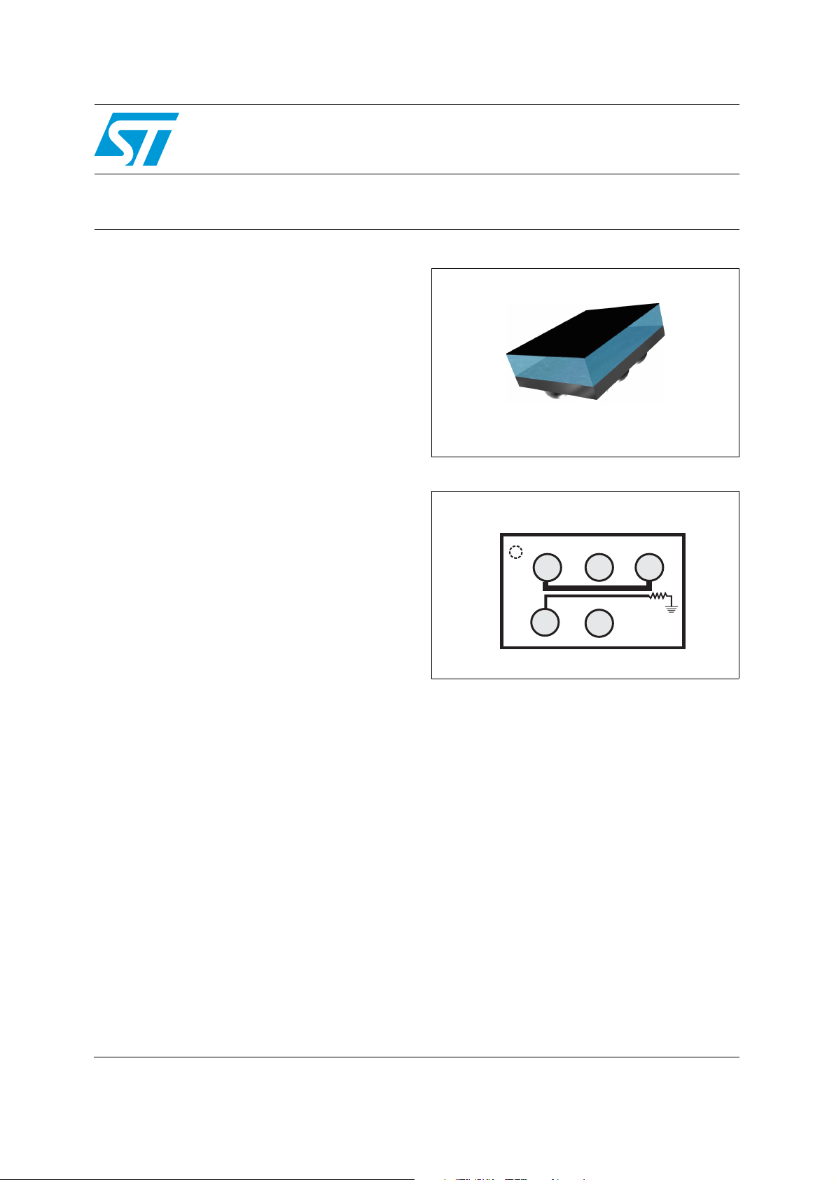
■ Packaged in Flip Chip
■ Package thickness: < 595 µm after reflow
■ Small footprint
CPL-WB-02D3
Wide-band, directional coupler
Datasheet − production data
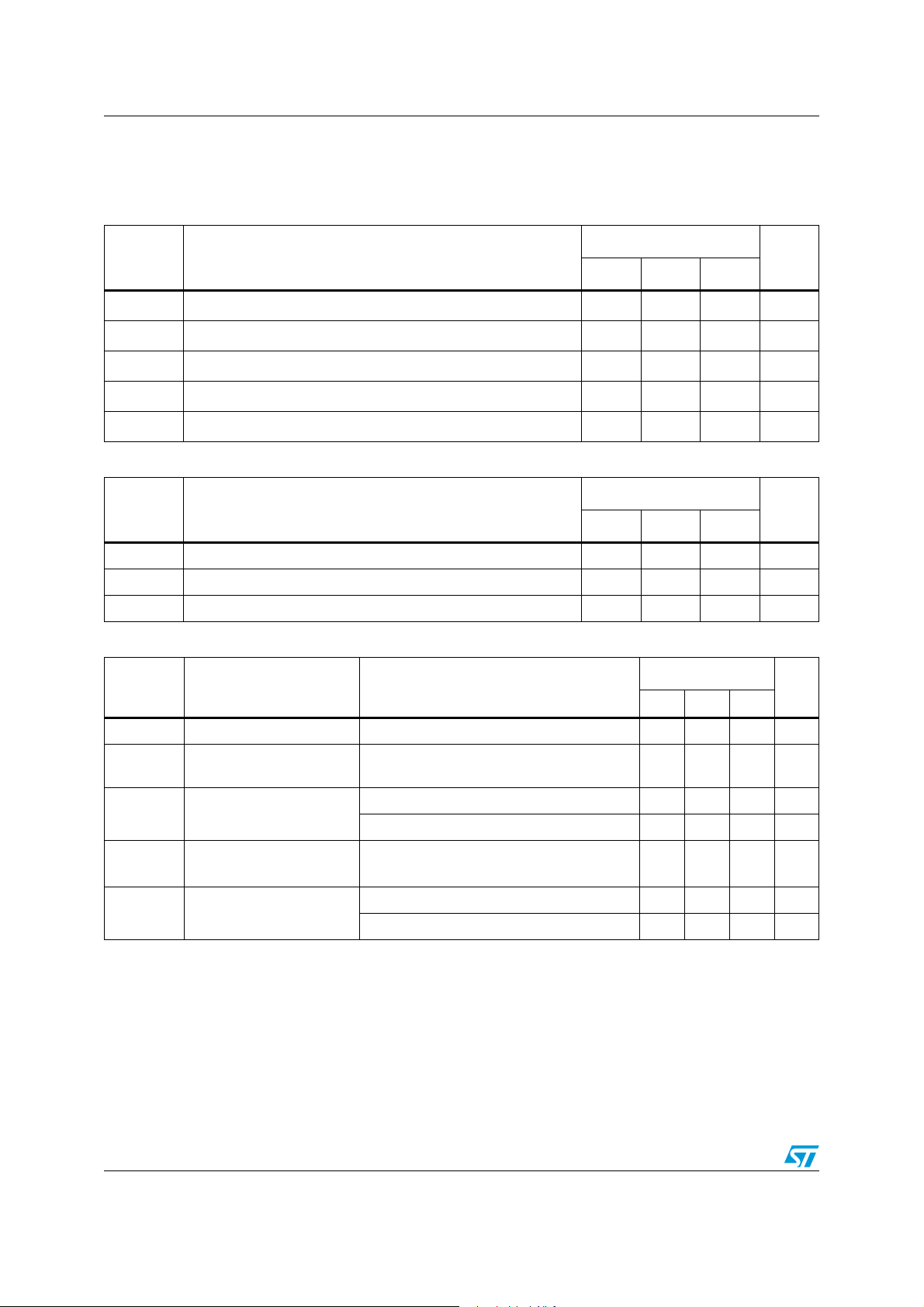
Flip Chip (5 bumps)
Figure 1. Pin configuration (bump view)
1
2
3
Benefits
■ Very low profile
■ Lead-free package
■ High RF performance
■ RF module size reduction
Applications
■ Quad-band power amplifier module
■ Quad-band front end module
■ WLAN
A
B
RF
CPLD
GND
IN
GND
RF
OUT
50 Ω
Description
The CPL-WB-02D3 is a wide-band directional
coupler designed to measure RF antenna output
power. This CPL has been customized for wide
band operating frequencies (2G/5G WLAN) with
low insertion losses in the transmit bandwidth
(2400 MHz to 5850 MHz).
The CPL-WB-02D3 has been designed using
STMicroelectronics IPD (integrated passive
device) technology on non-conductive glass
substrate to optimize RF performance. The device
is delivered 100% tested in tape and reel.
June 2012 Doc ID 023286 Rev 1 1/7
This is information on a product in full production.
www.st.com
7
Characteristics CPL-WB-02D3
1 Characteristics
Table 1. Absolute maximum rating (limiting values)
Symbol Parameter
P
V
ESD (HBM)
V
ESD (MM)
V
ESD (CDM)
T
OP
Table 2. Electrical characteristics (T
Input power RF
IN
IN
Human body model, JESD22-A114-B, All I/O 2 kV
Machine model, JESD22-A115-A, All I/O 100 V
Charge device model, JESD22-C101-C, All I/O 500 V
Operating temperature -30 +85 ºC
= 25 °C) - impedances
amb
Symbol Parameter
Z
OUT
Z
Z
CPLD
Table 3. Electrical characteristics (T
Nominal output impedance 50 Ω
Nominal input impedance 50 Ω
IN
Nominal coupling impedance 50 Ω
= 25 °C) - RF performance
amb
Symbol Parameter Test condition
T
OP
Operating temperature -30 +85 °C
Frequency range
f
(bandwidth)
From 2400 MHz to 2500 MHz 0.2 dB
I
R
Insertion loss in bandwidth
L
Return loss in bandwidth
L
(IN, OUT pins)
From 4900 MHz to 5850 MHz 0.5
From 2400 MHz to 5850 MHz 15 dB
From 2400 MHz to 2500 MHz 17 18 19 dB
CPLD Coupling factor
From 4900 MHz to 5850 MHz 11 12 13 dB
Value
Unit
Min. Typ. Max.
25 dBm
Value
Unit
Min. Typ. Max.
Value
Unit
Min. Typ. Max.
2400 5850 MHz
2/7 Doc ID 023286 Rev 1
CPL-WB-02D3 PCB recommendation
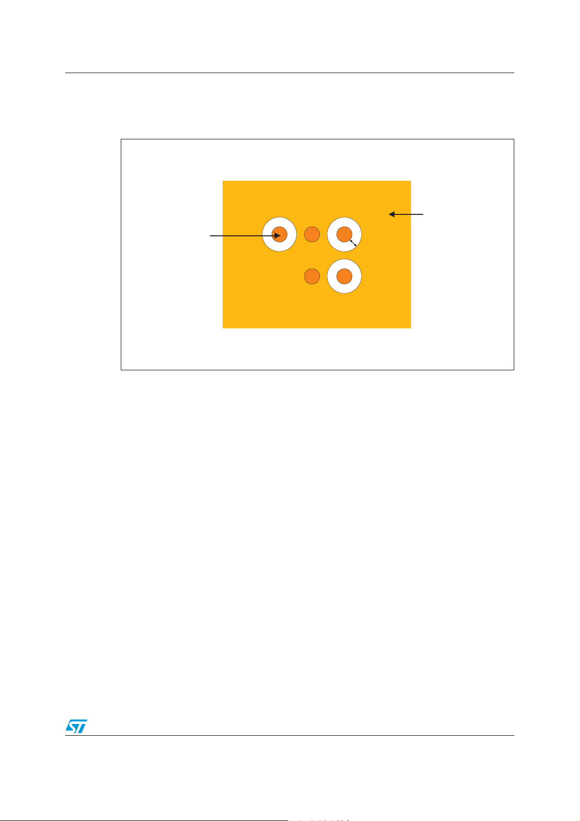
2 PCB recommendation
Figure 2. Recommended land pattern
Pads
Ø220 µm
OUT IN
GND
GND
CPL
Layer 1
Aperture
130 µm
Doc ID 023286 Rev 1 3/7
 Loading...