

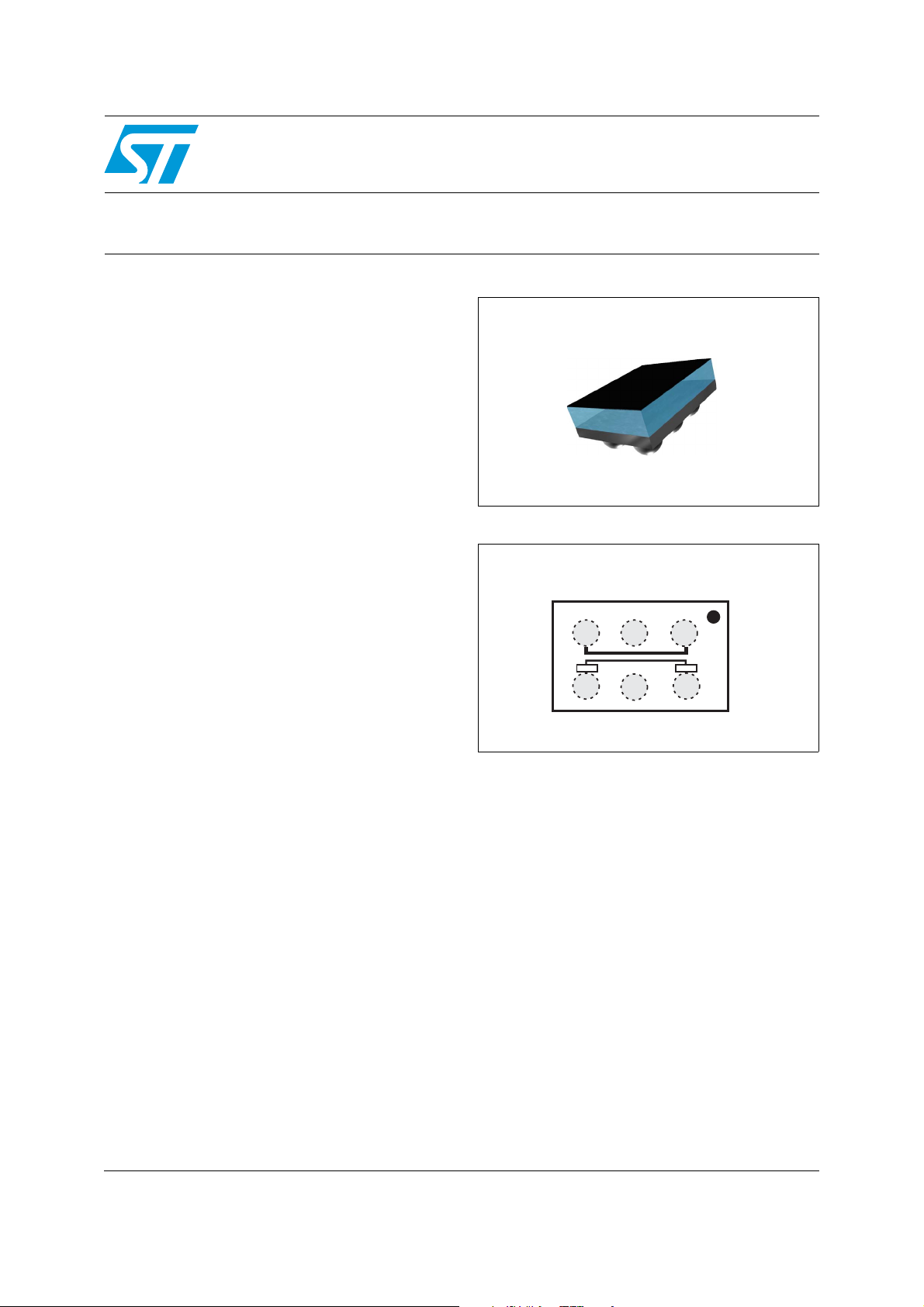
Wide band directional coupler with ISO port
Features
■ 50 Ω nominal input / output impedance
■ Wide operating frequency range
(824 MHz to 2170 MHz)
■ Low Insertion Loss (< 0.2 dB)
■ 34 dB typical coupling factor
■ High directivity (typical 25 dB)
■ High ESD robustness
(IEC 61000-4-2 Level 4)
■ Flip-Chip package
■ Small footprint: 1700 x 1200 µm
CPL-WB-00C2
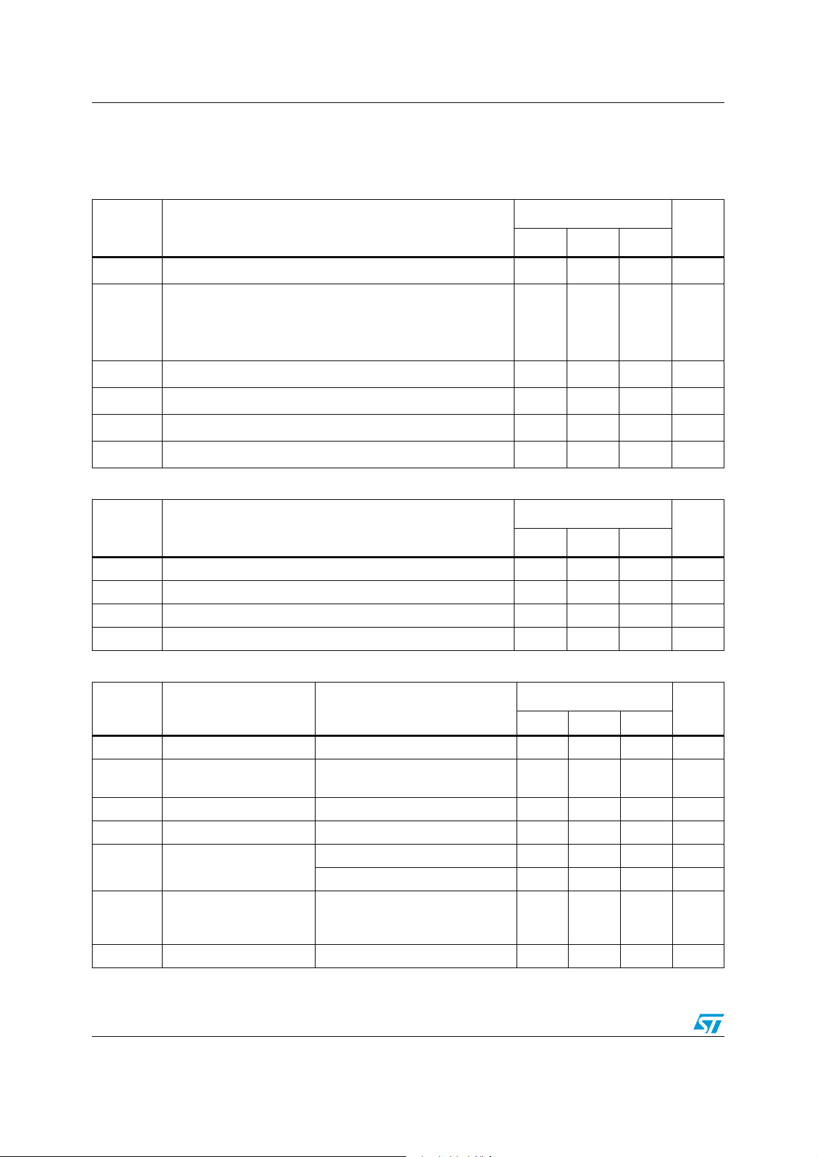
Figure 1. Pin configuration (top view)
Benefits
■ Very low profile (< 690 µm thickness)
■ Lead-free package
■ High RF performance
■ RF module size reduction
Applications
■ Quad band power amplifier module
■ Quad band front end module
■ GSM / WCDMA mobile phone
123
RF
GND
OUT
ATN. ATN.
ISO
GND
CPLD
RF
IN
A
B
Description
The CPL-WB-00C2 is a wide band directional
coupler designed to measure RF antenna output
power in GSM / WCDMA applications. This CPL
has been customized for wide band operating
frequencies (EGSM and CELL, PCS, DCS,
WCDMA Band I) with less than 0.2 dB insertion
losses in the transmit bandwidth (824 MHz to
2170 MHz).
The CPL-WB-00C2 has been designed using
STMicroelectronics IPD (integrated passive
device) technology on non conductive glass
substrate to optimize RF performance. The device
is delivered 100% tested in tape and reel.
January 2010 Doc ID 15088 Rev 3 1/8
www.st.com
8
Characteristics CPL-WB-00C2
1 Characteristics
Table 1. Absolute maximum rating (limiting values)
Symbol Parameter
IN
Input Power RF
IN
P
ESD ratings IEC 61000-4-2 (C = 150 pF, R = 330 Ω, 10 shots
V
ESD (IEC)
V
ESD (HBM)
V
ESD (MM)
V
ESD (CDM)
T
OP
Table 2. Electrical characteristics (T
with both polarities and each condition, cumulative method)
RF
RF
IN
IN
, RF
, RF
, air discharge
OUT
, contact discharge
OUT
Human body model, JESD22-A114-B, All I/O 2 kV
Machine model, JESD22-A115-A, All I/O 100 V
Charge device model, JESD22-C101-C, All I/O 500 V
Operating temperature -30 +85 ºC
= 25 °C) - impedances
amb
Symbol Parameter
Z
OUT
Z
Z
CPLD
Z
OUT
Table 3. Electrical characteristics (T
Nominal output impedance 50 Ω
Nominal input impedance 50 Ω
IN
Nominal coupling impedance 50 Ω
Nominal ISO impedance 50 Ω
= 25 °C) - RF performance
amb
Symbol Parameter Test condition
T
OP
I
R
CPLD
Operating temperature -30 +85 °C
Frequency range
f
(bandwidth)
Insertion loss in bandwidth From 824 MHz to 2170 MHz 0.1 0.2 dB
L
Return loss in bandwidth From 824 MHz to 2170 MHz 15 dB
L
Coupling factor (including
attenuator)
From 824 MHz to 915 MHz 35 39 dB
From 1710 MHz to 1980 MHz 28 33 dB
Value
Unit
Min. Typ. Max.
35 dBm
±15
±8
kV
kV
Value
Unit
Min. Typ. Max.
Value
Unit
Min. Typ. Max.
824 2170 MHz
(824 to 849 MHz) (880 to 915 MHz)
(1710 to 1785 MHz) (1850 to
1910 MHz)(1920 to 1980 MHz)
0.5 dB
Ripple
Coupling ripple in
individual band
DIR Coupler directivity From 824 MHz to 1980 MHz 20 25 dB
2/8 Doc ID 15088 Rev 3
CPL-WB-00C2 Characteristics
1.1 RF measurement (on reference evaluation board)
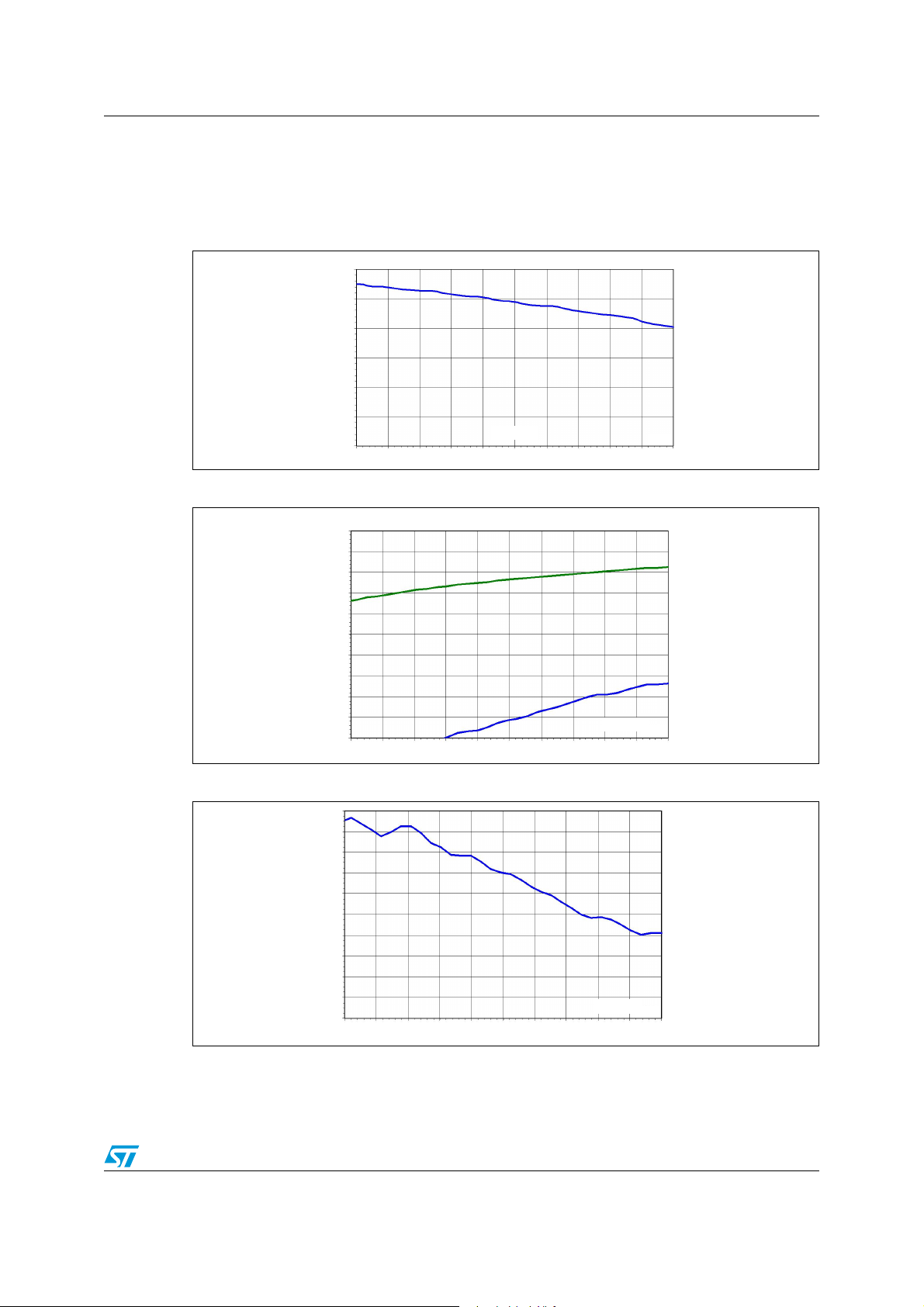
Measurements done on reference evaluation board under 50 Ω, de-embedding at
CPL-WB-00C2 bumps.
Figure 2. Insertion loss
dB
-0.0
-0.05
-0.1
-0.15
-0.2
-0.25
-0.3
Figure 3. Coupling and isolation
dB
-20
-25
-30
-35
-40
-45
-50
-55
-60
-65
-70
F (MHz)
20351901176616321497136212281093959824
F (MHz)
20351901176616321497136212281093959824
2170
2170
Figure 4. Directivity
40
38
36
34
32
30
28
26
24
22
20
F (MHz)
2170
20351901176616321497136212281093959824
Doc ID 15088 Rev 3 3/8
 Loading...