

based on the STM32F103RE and TS4657
Features
■ STM32F103RE performance line
microcontroller
■ 16 MHz crystal unit
■ USB connector and ESD protection
■ Two LEDs driven by the microcontroller
■ Push button to control the firmware mode
■ TS4657 - single supply stereo digital audio line
driver with 2.2 V
– 16- to 24-bit audio data format stereo DAC,
32 to 48 kHz sample rate
2
–I
S, right or left-justified compatible digital
audio interface
■ TS2012 - filter-free stereo 2x2.8 W class D
audio power amplifier
■ TS4962 - 2.8 W filter-free mono class D audio
power amplifier
– Output available either through mono jack
connector or to on-board speaker
■ TS472 - very low noise microphone
preamplifier with 2.0 V bias output and active
low standby mode
– Single-ended output available for
connection to ADC of a microcontroller
■ On-board microphone and small speaker
■ RoHS compliant
capless outputs:
RMS
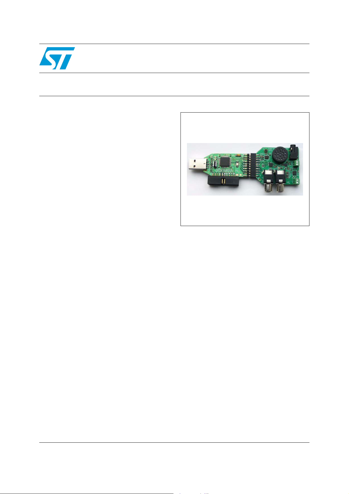
STEVAL-CCA021V1
USB audio demonstration board
Data brief
STEVAL-CCA021V1
Description
The STEVAL-CCA021V1 demonstration board
implements a USB audio card based on the
STM32F103RE microcontroller and the TS4657
audio digital-to-analog converter (decoder). The
complete system consists of a controller board
driven by the STM32F103RE microcontroller, and
a TS4657-based audio board.
Mono audio output is available either through the
TS4962-driven on-board speaker or via the mono
jack connector, and stereo output is possible
through the TS2012 stereo audio amplifier which
can drive external speakers. Both audio amplifiers
are class D.
For audio input, an on-board microphone is
connected through the TS472 microphone preamplifier to the ADC input of the microcontroller. It
is possible to disconnect the controller section
from the audio section to use the boards
September 2009 Doc ID 16318 Rev 1 1/5
For further information contact your local STMicroelectronics sales office.
individually for other applications.
www.st.com
5

Schematic diagrams STEVAL-CCA021V1
1 Schematic diagrams
Figure 1. Schematic diagram of the STM32F103RE-based controller board
LED_ACTIVE
A3V3
3V3
VSSA
12
VSSA
STM32F103RET6
13
C15
3V3
100nF
VSSA
2.3VLD1
LD2
GME 960-024
1 2
R13
220
R12
470
1
2
USB_ACTIVITY
C14
3V3
47
31
4
VSS_1
PC14-OSC32_IN
PC15-OSC32_OUT
VBAT
VDD_1
1
48
32
100nF
C13
100nF
C12
100nF
C11
100nF
R8
0R
18
VSS_363VSS_4
VSS_2
VDD_2
VDD_364VDD_419VDDA
I2C1_SDA
I2S2_CK
PA0PA1
PA2PA3
I2S2_MCK
I2S2_WS
I2S2_SD
I2C1_SCL
11 12
131415
PC1
PC2
PB759PB861PB9
BUTTON
16
17 18
PC0
62
29
43
3V3
19 20
BL220G
I2S2_CK
I2S2_WS
34
30
PB11
PB10
PB1233PB13
PA1245PA13/JTMS/SWDIO
PA11
44
46
49
JTCK
USBDN
JTMS
USBDP
3V3
PC0
PC1
PC2
I2S2_SD
36
10
PC08PC19PC2
PB1435PB15
OSC_IN/PD0
PA15/JTDI
OSC_OUT/PD1
PA14/JTCK/SWCLK
5
6
50
54
X2
JTDI
X1
R10
10k
PC3
11
PC3
PD2
60
BOOT0
R6
USB5V
4
10
7 8
1 2
3
5 6
9
P2
PC3
VSSA
A3V3
BOOT1
JTRST
I2C1_SCL
JTDO
I2C1_SDA
33pF
C10
X2
3
2
GND
GND
X1
TSX-3225 / 16MHz
1
4
33pF
C8
X1
56
58
28
27
55
57
PB026PB1
PB5
PB6
PB3/JTDO
PB2/BOOT1
PB4/JNTRST
PA0-WKUP
PA216PA3
PA521PA622PA723PA841PA942PA10
PA1
PA4
U1
15
20
14
17
PA1
PA0
PA2
PA3
SPI1_SCK
SPI1_MOSI
SPI1_NSS
SPI1_MISO
25
PC424PC5
BOOT0
10k
21
BUTTON
I2S2_MCK
37
PC738PC839PC9
PC6
NRST
7
NRST
C9
C7
100nF
B1
USB_ACTIVITY
LED_ACTIVE
52
51
40
PC11
PC10
100nF
53
2
3
PC12
PC13-TAMPER-RTC
USBDN
USBDP
USB5V
R4 4R7
USB1X90A PCB
USB5V
USB_A
R5 4R7
4
6
5
I/O1
I/O2
Vbus
I/O2
GND
I/O1
U4
2
3
1
1
2
4
3
D-
D+
Vbus
GND
1uF
C3
3V3USB5V
C1
4.7uF
10nF
C4
4
5
Vout
BYPASS
Vin
GND2INHB
U2
1
LD3985XX33
3
C5
4.7uF
1uF
C2
CN2
2/5 Doc ID 16318 Rev 1
10mH
L1
R14 10K
DBGACK
Inductor
3V3
SPI1_MOSI
SPI1_SCK
3V3
3
4
5
6
C
D
W
VSS
HOLD
Q
VCC8S
U3
C16
100nF
3V3
3V3
M25P64-VME6G
7
1
2
R9
10K
SPI1_NSS
SPI1_MISO
3V3
R3 1k5
USBLC6-2P6
Internal pull-up
R7 1M
C6 4.7nF
6
5
SH1
SH2
JTRST
3V3
1
234
CN1
MLW20G
Internal pull-up
JTDI
678
5
Internal pull-up
JTMS
pull-down
Internal
R1
JTCK
RTCK
9
11
10
10K
12
JTDO
131415
NRST
16
R2 10K
DBGRQ
17
181920

STEVAL-CCA021V1 Schematic diagrams
k
Figure 2. Schematic circuit of the TS4657-based audio board
Bloc
2
1
Terminal
P2
100pF
C8
C9
CC
CC
CC
10K
R2
10K
R1
L2
BLM18EG221SN1
5
2
LOUT+
LOUT-
H
PV
PV
PWM
AV
Gain
+
LIN
17
16
C11
220n
GND
100pF
BLM18EG221SN1
Bridge
Select
LIN -
G0
15
G0
C12
GND
L1
U2
ST: TS2012IQT
Stereo Class D Amplier
5V0
C7
C6
1uF
C5
1uF
13
100nF
34
5V0 5V05V0
GND GND
9
GND
Control
GND
GND Gain
J1
RCA WBTOR 1
GND
Oscillator
G1
1
G1
220n
100pF
C13
GND
C30
L3
14
ROUT+
H
Gain
RIN +
20
2
P3
BLM18EG221SN1
11
ROUT-
Bridge
PWM
Select
-
RIN
19
220n
GND
1
L4
C15
Terminal Block
C31
BLM18EG221SN1
Standby
STBY L
STBY R
8
7
STBY_R
STBY_L
220n
J3
100pF
Control
GND
RCA WBTOR 1
E-PAD
PGND
PGND
AGND
GND
R10
R9
External
21
12
18
Channel Standby
10K
10K
GND GND
Speakers
GND
5V0
GND GND
1503 06
J4
Lumberg
GND
Mono Jack
U3
9
7
6
300K
Mono Class D Amplier
10K
R13
GND
C32
100pF
L5
E-PAD
GNDA
VCCA
Bias
Internal
STBY
143
R14
SPK_STBY
C21
BLM18EG221SN1
5
OUT+
150K
150k
IN+
100nF
H
OUTPUT
PWM
R16
C22
IN-
L6
BRIDGE
8
OUT-
150K
150k
100nF
1
2
C33
100pF
BLM18EG221SN1
Oscillator
5V0
GND
GND
U6
C24
NC
100nF
C25
1uF
KSSG1708
Speaker
2
GND GND
ST: TS4962IQT
STEVAL-CCA021V1
TS4657 Audio Card
GNDA
coupling
DC
resistor for
MICRO_OUT
0R
R3
100K
Assembly
68
0R/22nF
C28
17
OUT+
C2
C1
Vcc
C19
1K
R11
R17
C28:
16
OUT-
IN+
IN-
5
8
C20
100nF
1
2
U5
100nF
GNDA
C29
1uF
9
GAIN
G
1K
R12
KEEG1542PBL
GNDA
2
BYPS
Bias
10
MICRO_SHDN
R15
10K
21
STBY
Bias
GND
GND
2.0V
GNDA
4
22
TS472IQT
ST:
GNDA
GNDA
Microphone Pre-Amplier
GND
2n2
C10
R4
U1
GND
C4
1uF
14
VREGA
18
5V0
P1
GND
1uF
GND
1uF
19
13
1uF
GND
G0
G1
123 4
MICRO_OUT
MICRO_SHDN
DAC_BCLK
DAC_LRCLK
5 6
7 8
9 10
VCCA
GNDA
VREGD
LDO
VCCD
VCCA
NCP
DAC_SDAT
DAC_MCLK
DAC_FMT2
131415
11 12
STBY_R
STBY_L
DAC_STBY
DAC_FMT1
16
17 18
SPK_STBY
DAC
C3
C2
5V0
5V0
C1
Connector
Board
Controller
820
12
Lout
DAC
LDO
PCP
19 20
Digital
Filters
Audio
Digital
BCLK
SDAT
LRCLK
3
DAC_BCLK
DAC_SDAT
DAC_LRCLK
R6
680
5V0
GND
10uF/16V
C26
5V0
GND
C16
100nF
R5
11
Rout
Interface
MCLK
654
DAC_MCLK
LED1
5V0
GND
2n2
C14
820
E-PAD
21
GNDD
17
GNDA
16
GNDA
15
GND
GNDA
10
GNDD
DAC
C35
C34
FMT2
7
DAC_FMT2
LED_RED_0805
10uF/16V
Interface
Control
GND
100nF
FMT1
8
DAC_FMT1
5V0
GND
STDBY
C36
1
2
20
9
R8
R7
R20
10K
10K
10uF/16V
GND
10K
DAC_STBY
GND
GND
GND
C18
VCCA
Microphone
GNDA
U4
100pF
C23
100pF
14
15
20
VCCA
100nF
C17
GNDA
1uF
C27
Doc ID 16318 Rev 1 3/5

Revision history STEVAL-CCA021V1
2 Revision history
Table 1. Document revision history
Date Revision Changes
29-Sep-2009 1 Initial release.
4/5 Doc ID 16318 Rev 1

STEVAL-CCA021V1
Please Read Carefully:
Information in this document is provided solely in connection with ST products. STMicroelectronics NV and its subsidiaries (“ST”) reserve the
right to make changes, corrections, modifications or improvements, to this document, and the products and services described herein at any
time, without notice.
All ST products are sold pursuant to ST’s terms and conditions of sale.
Purchasers are solely responsible for the choice, selection and use of the ST products and services described herein, and ST assumes no
liability whatsoever relating to the choice, selection or use of the ST products and services described herein.
No license, express or implied, by estoppel or otherwise, to any intellectual property rights is granted under this document. If any part of this
document refers to any third party products or services it shall not be deemed a license grant by ST for the use of such third party products
or services, or any intellectual property contained therein or considered as a warranty covering the use in any manner whatsoever of such
third party products or services or any intellectual property contained therein.
UNLESS OTHERWISE SET FORTH IN ST’S TERMS AND CONDITIONS OF SALE ST DISCLAIMS ANY EXPRESS OR IMPLIED
WARRANTY WITH RESPECT TO THE USE AND/OR SALE OF ST PRODUCTS INCLUDING WITHOUT LIMITATION IMPLIED
WARRANTIES OF MERCHANTABILITY, FITNESS FOR A PARTICULAR PURPOSE (AND THEIR EQUIVALENTS UNDER THE LAWS
OF ANY JURISDICTION), OR INFRINGEMENT OF ANY PATENT, COPYRIGHT OR OTHER INTELLECTUAL PROPERTY RIGHT.
UNLESS EXPRESSLY APPROVED IN WRITING BY AN AUTHORIZED ST REPRESENTATIVE, ST PRODUCTS ARE NOT
RECOMMENDED, AUTHORIZED OR WARRANTED FOR USE IN MILITARY, AIR CRAFT, SPACE, LIFE SAVING, OR LIFE SUSTAINING
APPLICATIONS, NOR IN PRODUCTS OR SYSTEMS WHERE FAILURE OR MALFUNCTION MAY RESULT IN PERSONAL INJURY,
DEATH, OR SEVERE PROPERTY OR ENVIRONMENTAL DAMAGE. ST PRODUCTS WHICH ARE NOT SPECIFIED AS "AUTOMOTIVE
GRADE" MAY ONLY BE USED IN AUTOMOTIVE APPLICATIONS AT USER’S OWN RISK.
Resale of ST products with provisions different from the statements and/or technical features set forth in this document shall immediately void
any warranty granted by ST for the ST product or service described herein and shall not create or extend in any manner whatsoever, any
liability of ST.
ST and the ST logo are trademarks or registered trademarks of ST in various countries.
Information in this document supersedes and replaces all information previously supplied.
The ST logo is a registered trademark of STMicroelectronics. All other names are the property of their respective owners.
© 2009 STMicroelectronics - All rights reserved
Australia - Belgium - Brazil - Canada - China - Czech Republic - Finland - France - Germany - Hong Kong - India - Israel - Italy - Japan -
STMicroelectronics group of companies
Malaysia - Malta - Morocco - Philippines - Singapore - Spain - Sweden - Switzerland - United Kingdom - United States of America
www.st.com
Doc ID 16318 Rev 1 5/5
 Loading...