2 W stereo audio power amplifier based on the TS4982
Features
■ 2 W output power into 4 Ω load per channel
■ 125 mW into 16 Ω load ground-referenced
stereo headphone driver
■ Four-step gain settings on speaker path
■ 3 levels of 3D effect on speaker path
■ PC-beep input system detection
■ ±8 kV HBM ESD-protected headphone outputs
■ Pop and click reduction circuitry
■ 32-pin 5 x 5 mm QFN package
■ Thermal shutdown and output short-circuit
protection
■ RoHS compliant
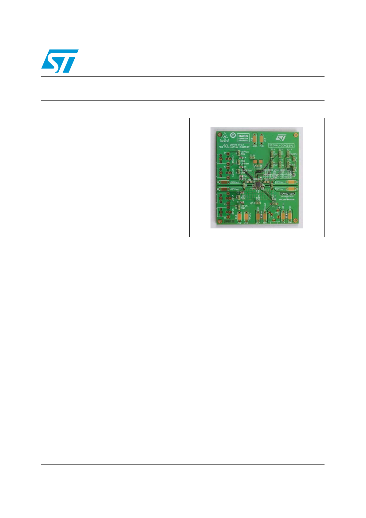
STEVAL-CCA019V1
Data brief
STEVAL-CCA019V1
AM05060v1
Description
The STEVAL-CCA019V1 is a demonstration
board designed to help in the characterization of
the TS4982, which features a stereo loudspeaker
driver and a ground-referenced stereo
headphones driver. An independent standby
mode pin allows the TS4982 to simultaneously
drive both output drivers.
Operating on a single 5 V supply, the TS4982
delivers 2 W (typ.) output power into a 4 Ω load at
1% THD+N.
The TS4982 features a PC beep input, three
levels of 3D stereo enhancement and 4-step gain
control using two digital input pins.
A minimum number of external components
makes the TS4982 well suited for notebook and
other hand-held sound equipment. It also has an
internal thermal shutdown (150° C) and output
short-circuit protection mechanism. The TS2012
is available in a 4x4 mm QFN20 package.
July 2009 Doc ID 16074 Rev 1 1/4
For further information contact your local STMicroelectronics sales office.
www.st.com
4

Schematic diagram STEVAL-CCA019V1
1 Schematic diagram
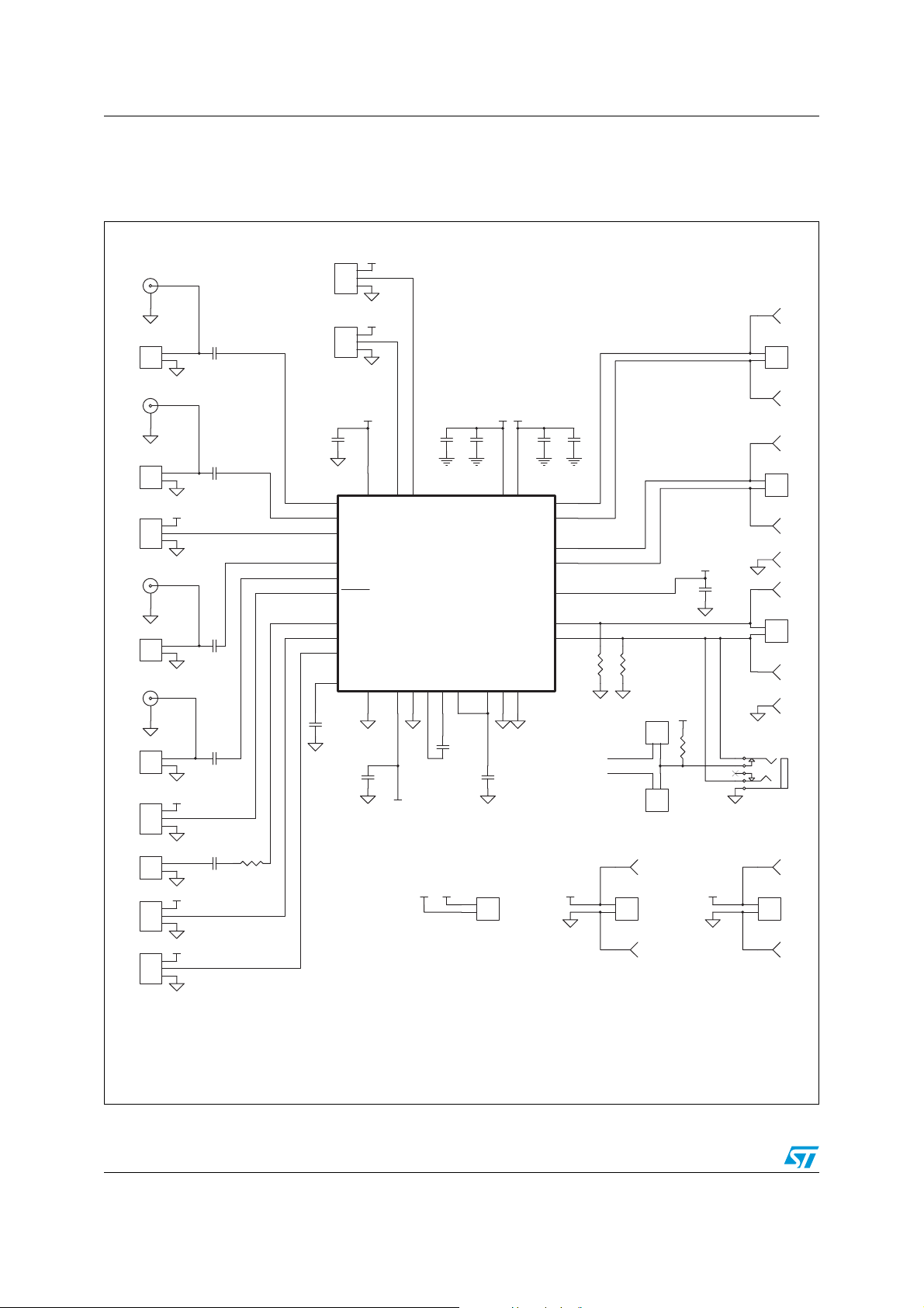
Figure 1. Circuit schematic
JP3
VCC
J1
N.A.
JP5
1
2
LHPin
J2
N.A.
JP6
1
2
RHPin
VCC
JP8
1
2
3
HDEN
J3
N.A.
JP10
1
2
LSPKin
J4
N.A.
JP12
1
2
RSPKin
JP13
VCC
1
2
3
SPKREN
JP14
1
2
PCBEEPin
VCC
JP4
1
2
3
G0
JP2G1VCC
1
2
3
C1
330nF
C2
330nF
HDEN
SPKREN
C3
330nF
C4
330nF
R1
C6
47k
330nF
1
2
3
3D1
VCC
JP1
1
2
3
3D0
VCC
C13
1uF
30
1
27
HLIN
26
HRIN
22
HDEN
3
LLIN
2
LRIN
23
SPKREN
4
BEEP
31
G0
32
G1
24
BYP
C14
1uF
C17
1uF
29
3D0
3D1
VCC
TS4982
CPVCC
GND
9
28
HPVCC
CP-
CP+10CPGND
11
12
HPVCCVCC
VCC VCC
C7C8
100nF
CPVSS
13
C5
1uF
JP18
2
1
C10 C11
Fn001.A.N
N.A.
PGND PGNDPGNDPGND
8
18
U1
20
ROUT+
19
ROUT-
PVCCL
PVCCR
6
LOUT+
7
LOUT-
17
HPVCC
16
LHP
15
RHP
R3
10kR210k
PGNDR
PVSS
PGNDL
5
21
14
C15
1uF
HPVCC
HDEN
SPKREN
JP16
1
2
JP19
JP20
J10
N.A.
J12
N.A.
HPVCC
C16
1uF
VCC
2
1
R4
100k
1
2
VCC
J5
N.A.
JP7
1
2
RSPKout
J6
N.A.
J7
N.A.
JP9
1
2
LSPKout
J8
N.A.
J16
N.A.
J14
N.A.
JP11
1
2
HPout
J15
N.A.
J17
N.A.
J9
N.A.
J11
N.A.
JP15
1
2
Vcc
J13
N.A.
2/4 Doc ID 16074 Rev 1
Comment: N.A. ... Not Assembled
AM05059V1
AM05060v1

STEVAL-CCA019V1 Revision history
2 Revision history
Table 1. Document revision history
Date Revision Changes
23-Jul-2009 1 Initial release.
Doc ID 16074 Rev 1 3/4

STEVAL-CCA019V1
y
y
Please Read Carefully:
Informatio n in this document is provided solely in connection with ST products. STMicroelectronics NV and its subsidiaries (“ST”) reserve the
right to make changes, corrections, modifications or improvements, to this document, and the products and services described herein at an
time, without notice.
All ST products are sold pursuant to ST’s terms and conditions of sale.
Purchasers are solely responsible for the choice, selection and use of the ST products and services described herein, and ST assumes no
liability whatsoever relating to the choice, selection or use of the ST products and services described herein.
No license, express or implied, by estoppel or otherwise, to any intellectual property rights is granted under this document. If any part of this
document refers to any third party products or services it shall not be deemed a license grant by ST for the use of such third party products
or services, or any intellectual property contained therein or considered as a warranty covering the use in any manner whatsoever of such
third party products or services or any intellectual property contained therein.
UNLESS OTHERWISE SET FORTH IN ST’S TERMS AND CONDITIONS OF SALE ST DISCLAIMS ANY EXPRESS OR IMPLIED
WARRANTY WITH RESPECT TO THE USE AND/OR SALE OF ST PRODUCTS INCLUDING WITHOUT LIMITATION IMPLIED
WARRANTIES OF MERCHANTABILITY, FITNESS FOR A PARTICULAR PURPOSE (AND THEIR EQUIVALENTS UNDER THE LAWS
OF ANY JURISDICTION), OR INFRINGEMENT OF ANY PATENT, COPYRIGHT OR OTHER INTELLECTUAL PROPERTY RIGHT.
UNLESS EXPRESSLY APPROVED IN WRITING BY AN AUTHORIZED ST REPRESENTATIVE, ST PRODUCTS ARE NOT
RECOMMENDED, AUTHORIZED OR WARRANTED FOR USE IN MILITARY, AIR CRAFT, SPACE, LIFE SAVING, OR LIFE SUSTAINING
APPLICATIONS, NOR IN PRODUCTS OR SYSTEMS WHERE FAILURE OR MALFUNCTION MAY RESULT IN PERSONAL INJURY,
DEATH, OR SEVERE PROPERTY OR ENVIRONMENTAL DAMAGE. ST PRODUCTS WHICH ARE NOT SPECIFIED AS "AUTOMOTIVE
GRADE" MAY ONLY BE USED IN AUTOMOTIVE APPLICATIONS AT USER’S OWN RISK.
Resale of ST products with provisions different from the statements and/or technical features set forth in this document shall immediately void
any warranty granted by ST for the ST product or service described herein and shall not create or extend in any manner whatsoever, an
liability of ST.
ST and the ST logo a re trademarks or registered trademarks of ST in various countries.
Information in this document supersedes and replaces all information previously supplied.
The ST logo is a registered trademark of STMicroelectronics. All other names are the property of their respective owners.
© 2009 STMicroelectronics - All rights reserved
Australia - Belgium - Brazil - Canada - China - Czech Republic - Finland - France - Germany - Ho ng Kong - India - Israel - Italy - Japan -
STMicroelectronics group of companies
Malaysia - Malta - Morocco - Philippines - Singapore - Spain - Sweden - Switzerland - United Kingdom - United States of America
www.st.com
4/4 Doc ID 16074 Rev 1
 Loading...