

Features
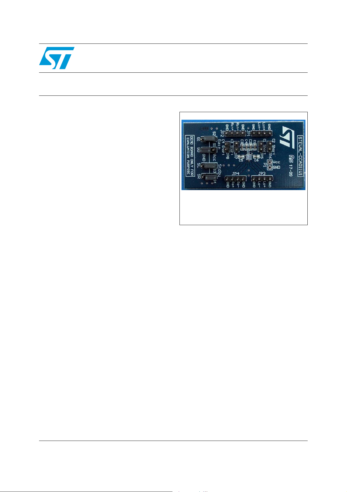
STEVAL-CCA011V1
Filter-free stereo 2x2.5 W Class-D audio power amplifier
demonstration board based on the TS2012FC
Data brief
■ Operating range from V
■ Dedicated standby mode active low for each
= 2.5 V to 5.5 V
CC
channel
■ Output power per channel: 1.15 W @5 V or
0.63 W @ 3.6 V into 8 Ω with 1% THD+N max
■ Output power per channel: 1.85 W @5 V into 4
Ω with 1% THD+N max
■ Output short-circuit protection
■ Four gain select settings: 6, 12, 18, 24 dB
■ Low current consumption
■ PSRR: 63 dB typ @ 217 Hz with 6 dB gain
■ Fast start-up phase: 8 ms
■ Thermal shutdown protection
■ RoHS compliant
Description
This demonstration board is based on TS2012FC
that is a fully differential Class-D stereo power
amplifier able to drive up to 1.15 W into an 8 Ω
load at 5 V per channel.
STEVAL-CCA011V1
It achieves better efficiency compared to typical
Class-AB audio amps.
The device has four different gain settings that
use two digital pins: G0 and G1. Pop and click
reduction circuitry provides low on/off switch noise
while allowing the device to start within 8 ms.
Two standby pins (active low) allow each channel
to be switched off independently.
The TS2012FC also integrates output shortcircuit protection and thermal shutdown protection
and it is available in a 16-bumps Flip-Chip
package.
June 2009 Doc ID 15789 Rev 1 1/6
For further information contact your local STMicroelectronics sales office.
www.st.com
6
Circuit schematics STEVAL-CCA011V1
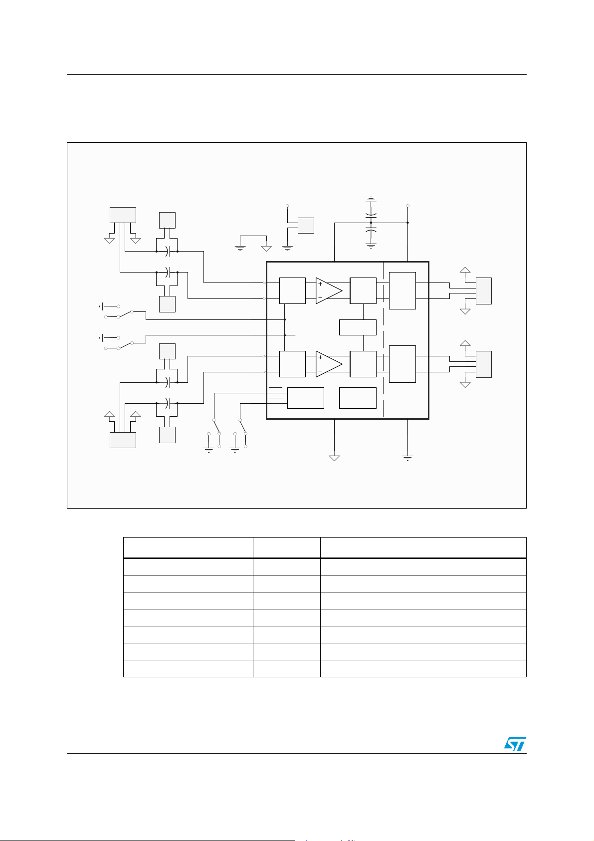
1 Circuit schematics
Figure 1. Schematic diagram
VCC
VCC
U1
Lin+
A1
Lin-
B1
G0
C2
G1
B2
Rin+
D1
Rin-
C1
STBYL
B4
STBYR
B3
TS2012 - FC16
Vcc
Gain
Select
Gain
Select
P1 Vcc
1
2
Standby
Control
AVCC
D2
C3
Vcc
Oscillator
Protection
PWM
PWM
Circuit
Lin+
Lin-
GND
GND
JP5
123
4
JP1
S1
3
2
1
G0
S2
3
2
1
G1
123
4
JP2
Rin+
Rin-
GND
GND
JP6
JP7
JP8
1
C1
220nF
C2
220nF
1
1
C3
220nF
C4
220nF
1
2
LinP
2
2
2
LinN
RinP
RinN
2
S3
STBL
1
3
VCC VCC
G0
G1
STBL
STBR
2
S4
STBR
1
3
100nF
C5
C6
1uF
PVCC
H
Bridge
H
Bridge
PGNDAGND
Vcc
Vcc
A2
A3
Lout+
A4
Lout-
Rout+
D3
Rout-
D4
C4
Pgnd
JP3
1
2
3
4
Header 4
JP4
1
2
3
4
Header 4
Table 1. Component list for the demonstration board
Designation Quantity Description
C1, C2, C3, C4 4 220 nF/16 V, SMD ceramic capacitor, 0603
C5 1 100 nF/16 V, SMD ceramic capacitor, 0603
C6 1 1 µF/16 V, SMD ceramic capacitor, 0603
P1, JP5, JP6, JP7, JP8 5 2-pin header 2.54 mm pitch
S1, S2, S3, S4 4 3-pin header 2.54 mm pitch
2/6 Doc ID 15789 Rev 1
JP1, JP2, JP3, JP4 4 4-pin header 2.54 mm pitch
U1 1 TS2012EIJT

STEVAL-CCA011V1 Demonstration board layout
2 Demonstration board layout
The following figures depict the top view and layers of the demonstration board.
Figure 2. PCB top layer Figure 3. PCB middle layer 1
Figure 4. PCB middle layer 2 Figure 5. PCB bottom layer
Doc ID 15789 Rev 1 3/6

Demonstration board layout STEVAL-CCA011V1
Figure 6. Top view and dimensions of the demonstration board
4/6 Doc ID 15789 Rev 1

STEVAL-CCA011V1 Revision history
3 Revision history
Table 2. Document revision history
Date Revision Changes
03-Jun-2009 1 Initial release.
Doc ID 15789 Rev 1 5/6

STEVAL-CCA011V1
Please Read Carefully:
Information in this document is provided solely in connection with ST products. STMicroelectronics NV and its subsidiaries (“ST”) reserve the
right to make changes, corrections, modifications or improvements, to this document, and the products and services described herein at any
time, without notice.
All ST products are sold pursuant to ST’s terms and conditions of sale.
Purchasers are solely responsible for the choice, selection and use of the ST products and services described herein, and ST assumes no
liability whatsoever relating to the choice, selection or use of the ST products and services described herein.
No license, express or implied, by estoppel or otherwise, to any intellectual property rights is granted under this document. If any part of this
document refers to any third party products or services it shall not be deemed a license grant by ST for the use of such third party products
or services, or any intellectual property contained therein or considered as a warranty covering the use in any manner whatsoever of such
third party products or services or any intellectual property contained therein.
UNLESS OTHERWISE SET FORTH IN ST’S TERMS AND CONDITIONS OF SALE ST DISCLAIMS ANY EXPRESS OR IMPLIED
WARRANTY WITH RESPECT TO THE USE AND/OR SALE OF ST PRODUCTS INCLUDING WITHOUT LIMITATION IMPLIED
WARRANTIES OF MERCHANTABILITY, FITNESS FOR A PARTICULAR PURPOSE (AND THEIR EQUIVALENTS UNDER THE LAWS
OF ANY JURISDICTION), OR INFRINGEMENT OF ANY PATENT, COPYRIGHT OR OTHER INTELLECTUAL PROPERTY RIGHT.
UNLESS EXPRESSLY APPROVED IN WRITING BY AN AUTHORIZED ST REPRESENTATIVE, ST PRODUCTS ARE NOT
RECOMMENDED, AUTHORIZED OR WARRANTED FOR USE IN MILITARY, AIR CRAFT, SPACE, LIFE SAVING, OR LIFE SUSTAINING
APPLICATIONS, NOR IN PRODUCTS OR SYSTEMS WHERE FAILURE OR MALFUNCTION MAY RESULT IN PERSONAL INJURY,
DEATH, OR SEVERE PROPERTY OR ENVIRONMENTAL DAMAGE. ST PRODUCTS WHICH ARE NOT SPECIFIED AS "AUTOMOTIVE
GRADE" MAY ONLY BE USED IN AUTOMOTIVE APPLICATIONS AT USER’S OWN RISK.
Resale of ST products with provisions different from the statements and/or technical features set forth in this document shall immediately void
any warranty granted by ST for the ST product or service described herein and shall not create or extend in any manner whatsoever, any
liability of ST.
ST and the ST logo are trademarks or registered trademarks of ST in various countries.
Information in this document supersedes and replaces all information previously supplied.
The ST logo is a registered trademark of STMicroelectronics. All other names are the property of their respective owners.
© 2009 STMicroelectronics - All rights reserved
Australia - Belgium - Brazil - Canada - China - Czech Republic - Finland - France - Germany - Hong Kong - India - Israel - Italy - Japan -
STMicroelectronics group of companies
Malaysia - Malta - Morocco - Philippines - Singapore - Spain - Sweden - Switzerland - United Kingdom - United States of America
www.st.com
6/6 Doc ID 15789 Rev 1
 Loading...