

ST BYW81HR User Manual
BYW81HR
Aerospace 1 x 15 A and 2 x 15 A - 200 V fast recovery rectifier
Features
■ Very small conduction losses
■ Negligible switching losses
■ High surge current capability
■ High avalanche energy capability
■ Hermetic packages
■ Target radiation qualification:
– 150 krad (Si) low dose rate
– 1 Mrad high dose rate
■ ESCC qualified
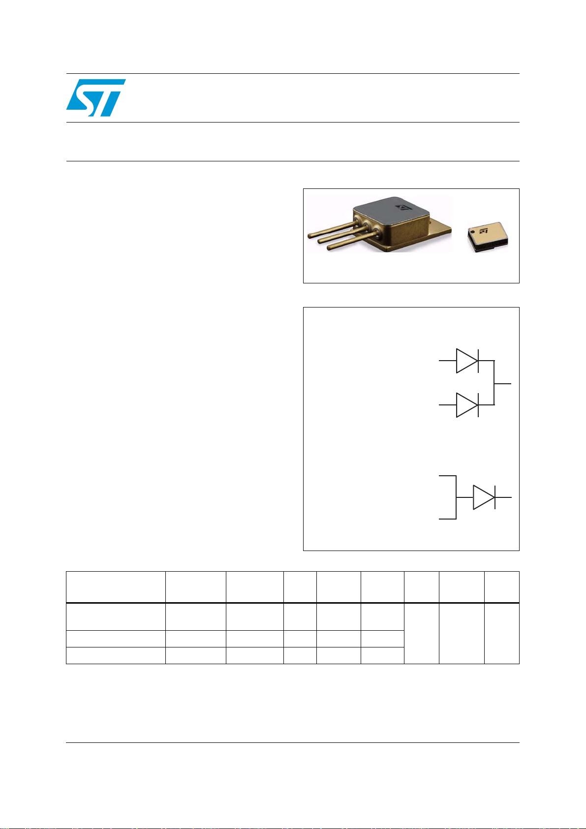
TO-254
Figure 1. Device configurations
Variant 03
BYW81-200CFSY1
SMD.5
Description
Packaged in hermetic TO-254 or SMD.5, this
device is intended for use in medium voltage, high
Terminal 1:
Terminal 2:
Terminal 3:
Anode a
Common cathode
Anode b
frequency switching mode power supplies, high
frequency DC to DC converters, and other
aerospace applications.
The case is not connected to any lead
The complete ESCC specification for this device
is available from the European Space Agency
web site. ST guarantees full compliance of
qualified parts with such ESCC detailed
specifications.
Terminal 1:
Terminal 2:
Terminal 3:
The lid is not connected to any terminal
Table 1. Device summary
Order code
BYW81-200CFSY1 -
(1)
ESCC part
number
Quality level EPPL Package I
Engineering
model
- TO-254 2 x 15 A
BYW81-200CFSYHRB 5103/029/03 ESCC flight - TO-254 2 x 15 A
BYW81-200SHRB 5103/029/05 ESCC flight Y SMD.5 15 A
1. Contact ST sales office for information about the specific conditions for products in die form and QML-Q versions.
Anode
Anode
Cathode
F(AV)
V
RRM
200 V 1.15 V 150 °C
1
3
Variant 05
BYW81-200SHRB
1
2
V
F (max)
T
j(max)
2
3
November 2010 Doc ID 17735 Rev 1 1/9
www.st.com
9

Characteristics BYW81HR
1 Characteristics
Table 2. Absolute maximum ratings
Symbol Characteristic Value Unit
(1) (2)
(5)
(3)
(2)
(5)
250
250
A
500
200 V
(2)(4)
15
15
A
30
30
30
A
40
-55 to +150 °C
-55 to +150 °C
+260
°C
+245
I
FSM
V
RRM
I
O
I
F(RMS)
T
OP
T
T
STG
T
SOL
Forward surge current
Variant 05
Variant 03 (per diode)
Variant 03 (per device)
Repetitive peak reverse voltage
Average output rectified current (50% duty cycle)
Variant 05
Variant 03 (per diode)
Variant 03 (per device)
Forward rms current (per diode)
Variant 05
Variant 03 (per diode)
Variant 03 (per device)
Operating case temperature range
Junction temperature +150 °C
J
Storage temperature range
Soldering temperature
(6)
TO-254
(7)
SMD.5
1. Sinusoidal pulse of 10 ms duration
2. For variant 03 the “per device” ratings apply only when both cathode terminals are tied together.
3. Pulsed, duration 5 ms, F = 50 Hz
4. For T
5. For devices with hot solder dip lead finish all testing performed at T
inert atmosphere.
6. Duration 10 seconds maximum at a distance of not less than 1.5 mm from the device body and the same
lead shall not be resoldered until 3 minutes have elapsed.
≥ +110°C, derate linearly to 0 A at +150°C.
case
> +125 °C are carried out in a 100%
amb
7. Duration 5 seconds maximum the same package shall not be resoldered until 3 minutes have elapsed.
Table 3. Thermal resistance
Symbol Parameter Value Unit
Junction to case
(1)
R
th (j-c)
1. Package mounted on infinite heatsink.
2. For variant 03 the “per device” ratings apply only when both cathode terminals are tied together.
All variants (per diode)
Variant 03 (per device)
(2)
2.3
1.4
°C/W
2/9 Doc ID 17735 Rev 1

BYW81HR Characteristics
Table 4. Electrical measurements at ambiant temperature (per diode), T
Symbol Characteristic
I
R
(1)
V
F1
(1)
V
F2
V
BR
C Capacitance 4001 V
t
rr
Z
th(j-c)
s
MIL-STD-750
test method
Test conditions
= 22 ±3 °C
amb
Limits
Min. Max.
Reverse current 4016 DC method, VR = 200 V - 20 µA
Forward voltage 4011
Pulse method, I
= 10 A - 1.0 V
F
Pulse method, IF = 20 A - 1.2 V
Breakdown voltage 4021 IR = 100 µA 200 - V
= 10 V, F = 1 MHz - 220 pF
R
I
= 1 A, VR = 30 V,
Reverse recovery time 4031
Relative thermal impedance,
(2)
junction to case
3101
F
/dt = -50 A/µs
dI
F
IH = 15 to 40 A, tH = 50 ms
= 50 mA, tmd = 100 µs
I
M
-40ns
Calculate ΔV
(3)
F
1. Pulse width ≤ 300µs, duty cycle ≤ 2%
2. Performed only during screening tests parameter drift values (initial measurements), go-no-go.
3. The limits for ΔVF shall be defined by the manufacturer on every lot in accordance with MIL-STD-750 Method 3101 and
shall guarantee the R
Table 5. Electrical measurements at high and low temperatures (per diode)
limits specified in maximum ratings.
th(j-c)
Units
°C/W
Limits
Min. Max.
-10mA
-0.85V
-1.15V
Symbol Characteristic
I
Reverse current 4016
R
(2)
V
Forward voltage 4011
F1
MIL-STD-750
test method
Test conditions
T
= +125 (+0, -5) °C
case
DC method, V
= +125 (+0, -5) °C
T
case
pulse method, I
= +55 (+0, -5) °C
T
case
pulse method, I
= 200 V
R
= 10 A
F
= 10 A
F
(1)
1. Read and record measurements shall be performed on a sample of 5 components with 0 failures allowed. Alternatively a
100% inspection may be performed.
2. Pulse width ≤ 300µs, duty cycle ≤ 2%
Units
Doc ID 17735 Rev 1 3/9
 Loading...