

BUL381
HIGH VOLTAGE FAST-SWITCHING
■ STMPREFERRED SALESTYPES
■ HIGH VOLTAGECAPABILITY
■ MINIMUMLOT-TO-LOT SPREADFOR
RELIABLEOPERATION
■ VERYHIGH SWITCHINGSPEED
■ FULLYCHARACTERISEDAT 125
APPLICATIONS
■ ELECTRONICBALLASTSFOR
FLUORESCENT LIGHTING
■ SWITCHMODEPOWERSUPPLIES
DESCRIPTION
The BUL381 and BUL382 manufactured using
high voltage Multiepitaxial Mesa technology for
cost-effective high performance. They use a
Hollow Emitter structure to enhance switching
speeds.
The BUL series is designed for use in lighting
applications and low cost switch-mode power
supplies.
o
C
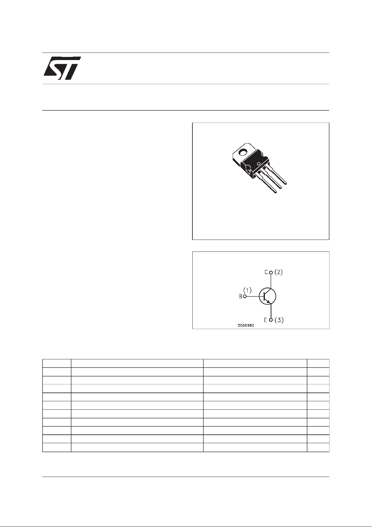
BUL382
NPN POWER TRANSISTOR
3
2
1
TO-220
INTERNAL SCHEMATIC DIAGRAM
ABSOLUTE MAXIMUM RATINGS
Symb o l Parame t er Val u e Uni t
V
V
V
I
I
P
T
June 1998
Collector-Emitter Voltage (VBE= 0) 800 V
CES
Collector-Emitter Voltage (IB= 0) 400 V
CEO
Emitter-Base Voltage (IC=0) 9 V
EBO
Collect or Current 5 A
I
C
Collect or Peak Current (tp<5ms) 8 A
CM
Base Current 2 A
I
B
Base Peak Current (tp<5ms) 4 A
BM
Total Dissipat ion at Tc=25oC70W
tot
Stora ge T emperature -65 to 150
stg
Max. Oper at i ng Junction T emperatur e 150
T
j
o
C
o
C
1/7
BUL381/ BUL382
THERMAL DATA
R
thj-case
R
thj-amb
Ther mal Resistance Ju nc t io n- Case Max
Thermal Resistance Junction-Ambient Max
1.78
62.5
o
C/W
o
C/W
ELECTRICAL CHARACTERISTICS (T
=25oC unlessotherwise specified)
case
Symbol Parameter Test C ondition s Min. Typ. Max. Unit
I
CES
I
CEO
V
CEO(sus)
Collector Cut-off
Current (V
BE
=0)
Collector Cut-off
Current (I
B
=0)
Collector-Em it t er
=800V
V
CE
V
=800V Tj=125oC
CE
V
=400V 250 µA
CE
100
500
IC= 100 mA L = 25 mH 400 V
Sust aining Voltage
V
V
CE(sat)
EBO
Emitt er-Base V oltage
=0)
(I
C
∗ Collector-Em it t er
Saturation Voltage
V
∗ Base-Emitt er
BE(sat)
Saturation Voltage
h
∗ DC C urr ent Gain IC=2A VCE=5V
FE
RESI STIVE LO AD
t
ON
t
s
t
f
Turn-on Time
St orage Time
Fall T ime
RESI STIVE LO AD
t
ON
t
s
t
f
Turn-on Time
St orage Time
Fall T ime
INDUCTIV E LOAD
t
s
t
f
St orage Time
Fall T ime
INDUCTIV E LOAD
t
∗
Pulsed: Pulse duration = 300 µs,duty cycle1.5 %
s
t
f
St orage Time
Fall T ime
I
=10mA 9 V
E
IC=1A IB=0.2A
=2A IB=0.4A
I
C
=3A IB=0.8A
I
C
IC=1A IB=0.2A
=2A IB=0.4A
I
C
0.5
0.7
1.1
1.1
1.2
8
=10mA VCE=5V
I
C
10
VCC=250 V IC=2A
I
=0.4A IB2=-0.4A
B1
(f or B UL 381only)
=30µs
t
p
1.4
1
2.2
800
VCC=250 V IC=2A
=0.4A IB2=-0.4A
I
B1
(f or B UL 382 only)
=30µs
t
p
1.7
1
2.5
800
IC=2A VCL= 250 V
=0.4A IB2=-0.8A
I
B1
L = 200 µH
1.7
75
2.6
120
IC=2A VCL= 250 V
=0.4A IB2=-0.8A
I
B1
L = 200 µHT
= 125oC
j
2.6
150
µA
µA
V
V
V
V
V
µs
µs
ns
µs
µs
ns
µs
ns
µs
ns
2/7

BUL381 / BUL382
Safe Operating Areas
DCCurrent Gain
DeratingCurves
DC Current Gain
CollectorEmitterSaturationVoltage
BaseEmitterSaturationVoltage
3/7

BUL381/ BUL382
ReverseBiased SOA InductiveFall Time
InductiveStorage Time InductiveFall Time
InductiveStorage Time Resistive Load SwitchingTest Ciurcuit
1) F a st el ec t ro nic s witch
2) No n-induc tive Resistor
4/7

ReverseBSOA and Inductive Load Switching
Test Ciurcuit
1) F as t e lec t r onic switc h
2) Non-in duc t i v e R esistor
3) Fast recovery Rectif ier
BUL381 / BUL382
5/7

BUL381/ BUL382
TO-220 MECHANICAL DATA
DIM.
MIN. TYP. MAX. MIN. TYP. MAX.
A 4.40 4.60 0.173 0.181
C 1.23 1.32 0.048 0.051
D 2.40 2.72 0.094 0.107
D1 1.27 0.050
E 0.49 0.70 0.019 0.027
F 0.61 0.88 0.024 0.034
F1 1.14 1.70 0.044 0.067
F2 1.14 1.70 0.044 0.067
G 4.95 5.15 0.194 0.203
G1 2.4 2.7 0.094 0.106
H2 10.0 10.40 0.393 0.409
L2 16.4 0.645
L4 13.0 14.0 0.511 0.551
L5 2.65 2.95 0.104 0.116
L6 15.25 15.75 0.600 0.620
L7 6.2 6.6 0.244 0.260
L9 3.5 3.93 0.137 0.154
DIA. 3.75 3.85 0.147 0.151
mm inch
6/7
P011C

BUL381 / BUL382
Information furnished is believed tobe accurate and reliable. However, STMicroelectronicsassumes no responsibility for theconsequences
of use of such information nor for any infringement of patents or other rights of third parties which may resultfrom its use. No license is
granted by implication orotherwiseunder any patent or patent rights of STMicroelectronics. Specification mentionedin this publication are
subject tochange withoutnotice. This publicationsupersedes and replaces all information previouslysupplied. STMicroelectronics products
are not authorized for use as critical componentsin life support devices or systems without express written approval of STMicroelectronics.
Australia - Brazil - Canada- China - France- Germany- Italy - Japan - Korea- Malaysia - Malta - Mexico - Morocco- TheNetherlands -
Singapore- Spain - Sweden- Switzerland- Taiwan -Thailand - United Kingdom- U.S.A.
The ST logo is a trademarkof STMicroelectronics
1998 STMicroelectronics – Printedin Italy – All Rights Reserved
STMicroelectronicsGROUP OF COMPANIES
.
7/7
 Loading...