

ST BTA08, BTB08 User Manual
BTA08, BTB08
T810, T835
Snubberless™, logic level and standard 8 A Triacs
Features
■ On-state rms current, I
■ Repetitive peak off-state voltage, V
600 to 800 V
■ Triggering gate current, I
T(RMS)
GT (Q1)
8 A
DRM/VRRM
5 to 50 mA
Description
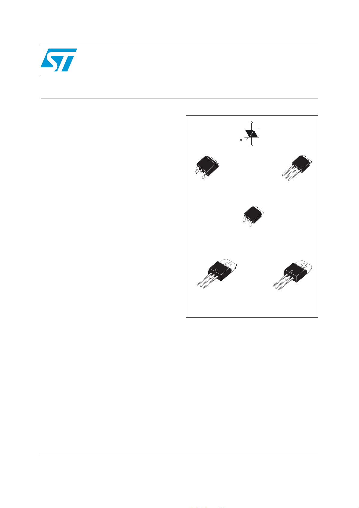
Available either in through-hole or surface-mount
packages, the BTA08, BTB08 and T8 triac series
is suitable for general purpose AC switching. They
can be used as an ON/OFF function in
applications such as static relays, heating
regulation, induction motor starting circuits... or
for phase control operation in light dimmers,
motor speed controllers,...
The snubberless versions (BTA/BTB...W and T8
series) are specially recommended for use on
inductive loads, thanks to their high commutation
performances.
Logic level versions are designed to interface
directly with low power drivers such as
microcontrollers.
By using an internal ceramic pad, the BTA series
provides voltage insulated tab (rated at 2500
V
) complying with UL standards (file ref.:
RMS
E81734).
A2
A2
A1
A2
G
D2PAK
(T8-G)
G
A1
A2
A1
A2
G
IPAK
(T8-H)
A2
A1
A2
G
DPAK
(T8-B)
A2
A1
A2
G
TO-220AB Insulated
(BTA08)
A1
A2
G
TO-220AB
(BTB08)
March 2010 Doc ID 7472 Rev 7 1/12
www.st.com
12

Characteristics BTA08, BTB08 and T8 Series
1 Characteristics
Table 1. Absolute maximum ratings
Symbol Parameter Value Unit
I
T(RMS)
On-state rms current (full sine wave)
IPAK/D2PAK/DPAK/
TO-220AB
= 110 °C
T
c
8A
TO-220AB Ins. Tc = 100 °C
I
dI/dt
Non repetitive surge peak on-state current
TSM
(full cycle, T
²
tI²t value for fusing tp = 10 ms 36 A²s
I
Critical rate of rise of on-state current I
x I
GT
,
initial = 25 °C)
j
G
F = 50 Hz t = 20 ms 80
F = 60 Hz t = 16.7 ms 84
= 2
F = 120 Hz Tj = 125 °C 50 A/µs
tr ≤ 100 ns
I
Peak gate current tp = 20 µs Tj = 125 °C 4 A
GM
P
T
Table 2. Electrical characteristics (Tj = 25 °C, unless otherwise specified)
Average gate power dissipation Tj = 125 °C 1 W
G(AV)
Storage junction temperature range
stg
T
Operating junction temperature range
j
- 40 to + 150
- 40 to + 125
Snubberless and logic level (3 quadrants)
T8 BTA08 / BTB08
Symbol Test conditions Quadrant
(1)
I
GT
V
V
I
H
VD = 12 V RL = 30 Ω
GT
VD = V
GD
= 125 °C
T
j
(2)
IT = 100 mA MAX. 15 35 10 15 35 50 mA
DRM RL
= 3.3 kΩ
I - II - III MAX. 10 35 5 10 35 50 mA
I - II - III MAX. 1.3 V
I - II - III MIN. 0.2 V
I - III
I
IG = 1.2 I
L
GT
II 30 60 15 30 60 80
T810 T835 TW SW CW BW
25 50 10 25 50 70
MAX.
Unit
A
°C
mA
dV/dt
(dI/dt)c
(2)
VD = 67 %V
(2)
Tj = 125 °C
(dV/dt)c = 0.1 V/µs Tj = 125 °C
Without snubber T
gate open
DRM
MIN. 40 400 20 40 400 1000 V/µs
5.4 - 3.5 5.4 - -
= 125 °C 2.8 - 1.5 2.98 - -
j
= 125 °C - 4.5 - - 4.5 7
j
MIN.
2/12 Doc ID 7472 Rev 7
A/ms(dV/dt)c = 10 V/µs T
BTA08, BTB08 and T8 Series Characteristics
Table 3. Standard (4 quadrants)
BTA08 / BTB08
Symbol Test conditions Quadrant
Unit
CB
(1)
I
GT
V
V
I
H
dV/dt
(dV/dt)c
Table 4. Static characteristics
VD = 12 V, RL = 33 Ω
GT
VD = V
GD
(2)
IT = 500 mA MAX. 25 50 mA
I
IG = 1.2 I
L
(2)
VD = 67 %V
(dI/dt)c = 5.3 A/ms Tj = 125 °C MIN. 5 10 V/µs
(2)
, RL = 3.3 kΩ, Tj = 125 °C ALL MIN. 0.2 V
DRM
GT
gate open Tj = 125 °C MIN. 200 400 V/µs
DRM
I - II - III
IV
MAX.
ALL MAX. 1.3 V
I - III - IV
MAX.
II 80 100
25
50
50
100
40 50
Symbol Test conditions Value Unit
(1)
V
TM
V
R
I
DRM
I
RRM
1. minimum IGT is guaranted at 5% of IGT max.
2. for both polarities of A2 referenced to A1.
Table 5. Thermal resistance
ITM = 11 A, tp = 380 µs Tj = 25 °C MAX. 1.55 V
(2)
Threshold voltage Tj = 125 °C MAX. 0.85 V
t0
(2)
Dynamic resistance Tj = 125 °C MAX. 50 mΩ
d
Tj = 25 °C
V
DRM
= V
RRM
= 125 °C 1 mA
T
j
MAX.
5µA
mA
mA
Symbol Parameter Value Unit
2
PAK / DPAK / TO-220AB 1.6
°C/W
°C/W
R
R
Junction to case (AC)
th(j-c)
Junction to ambient
th(j-a)
S = 1 cm
S = 0.5 cm
IPAK / D
TO-220AB Insulated 2.5
²
D2PA K 4 5
²
DPAK 70
TO-220AB / TO-220AB Insulated 60
IPAK 100
S = Copper surface under tab.
Doc ID 7472 Rev 7 3/12
Characteristics BTA08, BTB08 and T8 Series
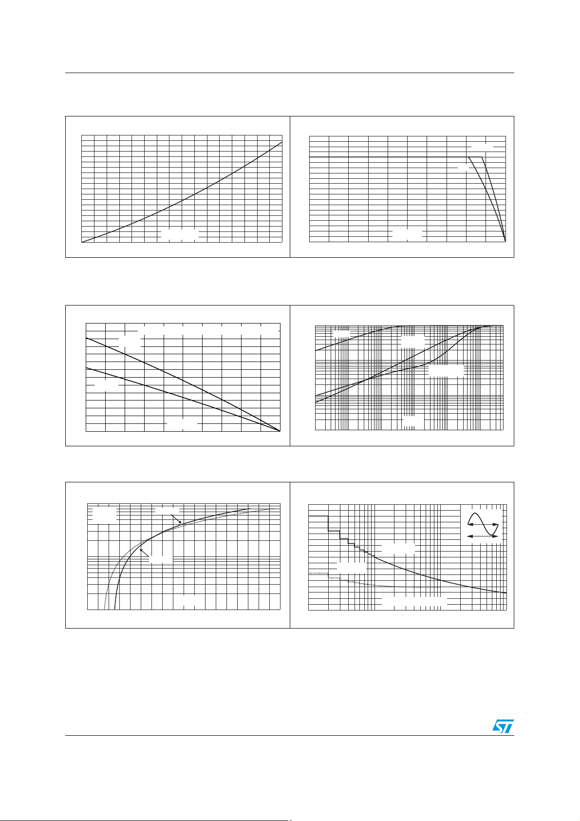
Figure 1. Maximum power dissipation versus
rms on-state current (full cycle)
P(W)
10
9
8
7
6
5
4
3
2
1
0
012345678
I (A)
T(RMS)
Figure 3. On-state rms current versus
ambient temperature (full cycle)
I (A)
T(RMS)
3.5
3.0
2.5
2.0
1.5
DPAK
(S=0.5CM )
1.0
0.5
0.0
0 25 50 75 100 125
printed circuit board FR4, copper thickness: 35 µm
2
DPAK
2
(S=1CM )
2
T (°C)
C
Figure 2. On-state rms current versus case
temperature (full cycle)
I (A)
T(RMS)
10
9
8
7
6
5
4
3
2
1
0
0 25 50 75 100 125
T (°C)
C
BTB / T8
BTA
Figure 4. Relative variation of thermal
impedance versus pulse
duration
K=[Z /R
1E+0
1E-1
1E-2
1E-3
1E-3 1E-2 1E-1 1E+0 1E+1 1E+2 5E+2
th th
Z
th(j-c)
]
DPAK/IPAK
Z
th(j-a)
2
TO-220AB/D PAK
Z
th(j-a)
t (s)
p
Figure 5. On-state characteristics
Figure 6. Surge peak on-state current
(maximum values)
I (A)
TM
100
T max.
j
V = 0.85V
to
Ω
R = 50 m
d
10
1
0.5 1.0 1.5 2.0 2.5 3.0 3.5 4.0 4.5 5.0
T=jT max.
T = 25°Cj.
j
V (V)
TM
4/12 Doc ID 7472 Rev 7
I (A)
TSM
90
80
70
60
50
40
30
20
10
0
1 10 100 1000
versus number of cycles
Non repetitive
T initial=25°C
j
Repetitive
T =110°C
C
Number of cycles
t=20ms
One cycle
 Loading...