

ST BTA24, BTB24, BTA25, BTA26, BTB26 User Manual
BTA24, BTB24, BTA25
BTA26, BTB26, T25
25 A standard and Snubberless™ triacs
Features
■ High current triac
■ Low thermal resistance with clip bonding
■ High commutation (4 quadrant) or very high
commutation (3 quadrant) capability
■ BTA series UL1557 certified (File ref: 81734)
■ Packages are RoHS (2002/95/EC) compliant
Applications
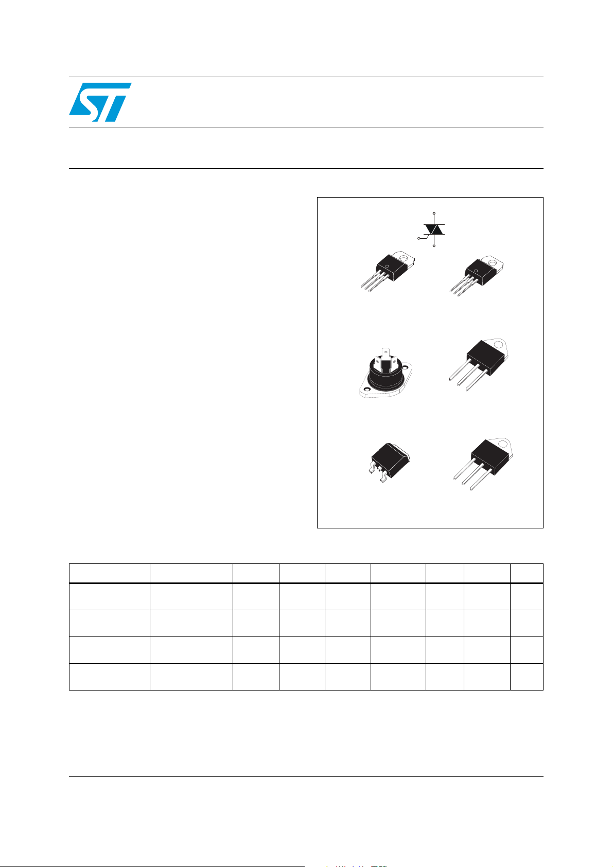
TO-220AB Insulated
Applications include the ON/OFF function in
applications such as static relays, heating
regulation, induction motor starting circuits, etc.,
or for phase control operation in light dimmers,
motor speed controllers, and silmilar.
The snubberless versions (BTA/BTB...W and T25
series) are especially recommended for use on
inductive loads, due to their high commutation
performances. The BTA series provides an
insulated tab (rated at 2500 V
RMS
).
Description
Available either in through-hole or surface-mount
packages, the BTA24, BTB24, BTA25, BTA26,
BTB26 and T25 triac series is suitable for general
purpose mains power AC switching.
Table 1. Device summary
Symbol Parameter BTA24
I
T(RMS)
V
DRM/VRRM
I
(Snubberless)
GT
(Standard)
I
GT
1. Insulated packages
2. 600 V version available only with IGT = 50 mA (Snubberless and Standard)
RMS on-state
current
Repetitive peak
off-state voltage
Triggering gate
current
Triggering gate
current
(1)
25 25 25 25 25 25 A
600 / 800 600 / 800 600 / 800 600
35 / 50 35 / 50 50 35 / 50 - 35 mA
-50505050-mA
BTB24 BTA25
A1
A2
G
(BTA24)
G
(BTA25)
A1
D2PAK
(1)
A1
RD91
A2
G
(T25)
BTA26
(2)
A2
A2
(1)
/ 800
A2
G
A1
A1
A2
G
TO-220AB
(BTB24)
A1
A2
G
TOP3 Insulated
(BTA26)
A1
A2
G
TOP3
(BTB26)
BTB26 T25 Unit
600 600 / 800 V
A2
A2
TM: Snubberless is a trademark of STMicroelectronics
July 2007 Rev 10 1/12
www.st.com
12
Characteristics BTA24, BTB24, BTA25, BTA26, BTB26, T25
1 Characteristics
Table 2. Absolute maximum ratings
Symbol Parameter Value Unit
TOP3 Tc = 105° C
2
D
I
T(RMS)
PAK /
TO-220AB
RMS on-state current (full sine wave)
RD91 Ins/
TOP3 Ins.
= 100° C
T
c
= 100° C
T
c
25 A
TO-220AB Ins. Tc = 75° C
I
TSM
²
I
dI/dt
V
DSM/VRSM
I
GM
P
G(AV)
T
stg
T
Table 3. Electrical characteristics (Tj = 25° C, unless otherwise specified), Snubberless and
Non repetitive surge peak on-state
current (full cycle, T
tI
²
t Value for fusing tp = 10 ms 340 A²s
initial = 25° C)
j
Critical rate of rise of on-state current
I
= 2 x IGT , tr ≤ 100 ns
G
Non repetitive surge peak off-state
voltage
Peak gate current tp = 20 µs Tj = 125° C 4 A
Average gate power dissipation Tj = 125° C 1 W
Storage junction temperature range
Operating junction temperature range
j
F = 50 Hz t = 20 ms 250
F = 60 Hz t = 16.7 ms 260
F = 120 Hz T
= 10 ms Tj = 25° C
t
p
= 125° C 50 A/µs
j
V
DRM/VRRM
+ 100
- 40 to + 150
- 40 to + 125
A
V
° C
logic level (3 quadrants) T25, BTA/BTB24...W, BTA25...W, BTA26...W
Symbol Test Conditions Quadrant
(1)
I
GT
V
GT
V
GD
(2)
I
H
I
L
dV/dt
(dI/dt)c
1. minimum IGT is guaranted at 5% of IGT max.
2. for both polarities of A2 referenced to A1.
VD = 12 V RL = 33 Ω
VD = V
= 125° C
T
j
RL = 3.3 kΩ
DRM
IT = 500 mA MAX. 50 50 75 mA
IG = 1.2 I
(2)
VD = 67 %V
(2)
Without snubber Tj = 125° C MIN. 13 13 22 A/ms
GT
gate open Tj = 125° C MIN. 500 500 1000 V/µs
DRM
I - II - III MAX. 35 35 50 mA
I - II - III MAX. 1.3 V
I - II - III MIN. 0.2 V
2/12
T25 BTA/BTB
T2535 CW BW
I - III
70 70 80
MAX.
II 80 80 100
Unit
mA
BTA24, BTB24, BTA25, BTA26, BTB26, T25 Characteristics
Table 4. Electrical characteristics (Tj = 25° C, unless otherwise specified),
standard (4 quadrants), BTB24...B, BTA25...B, BTA26...B, BTB26...B
Symbol Test Conditions Quadrant Value Unit
(1)
I
GT
I
V
GT
V
GD
(2)
H
VD = 12 V RL = 33 Ω
VD = V
RL = 3.3 kΩ Tj = 125° C ALL MIN. 0.2 V
DRM
)IT = 500 mA MAX. 80 mA
I - II - III
MAX.
IV 100
ALL MAX. 1.3 V
I - III - IV
I
L
dV/dt
(dV/dt)c
1. minimum IGT is guaranted at 5% of IGT max.
2. for both polarities of A2 referenced to A1.
Table 5. Static characteristics
IG = 1.2 I
(2)
VD = 67 %V
(2)
(dI/dt)c = 13.3 A/ms Tj = 125° C MIN. 10 V/µs
GT
II 160
gate open Tj = 125° C MIN. 500 V/µs
DRM
MAX.
Symbol Test Conditions Value Unit
(1)
V
TM
V
t0
R
d
I
DRM
I
RRM
1. for both polarities of A2 referenced to A1.
ITM = 35 A tp = 380 µs Tj = 25° C MAX. 1.55 V
(1)
Threshold voltage Tj = 125° C MAX. 0.85 V
(1)
Dynamic resistance Tj = 125° C MAX. 16 mΩ
Tj = 25° C
V
DRM
= V
RRM
= 125° C 3 mA
T
j
MAX.
50
70
5µA
mA
mA
Table 6. Thermal resistance
Symbol Parameter Value Unit
TOP 3 0.6
2
D
R
th(j-c)
Junction to case (AC)
PAK / TO-220AB 0.8
RD91 Insulated / TOP3 Insulated 0.9
TO-220AB Insulated 1.7
R
th(j-a)
Junction to ambient
(1)
S = 1 cm
²
D2PA K 4 5
TO-220AB / TO-220AB Insulated 60
1. S = Copper surface under tab.
3/12
° C/W
° C/WTOP3 / TOP3 Insulated 50
Characteristics BTA24, BTB24, BTA25, BTA26, BTB26, T25
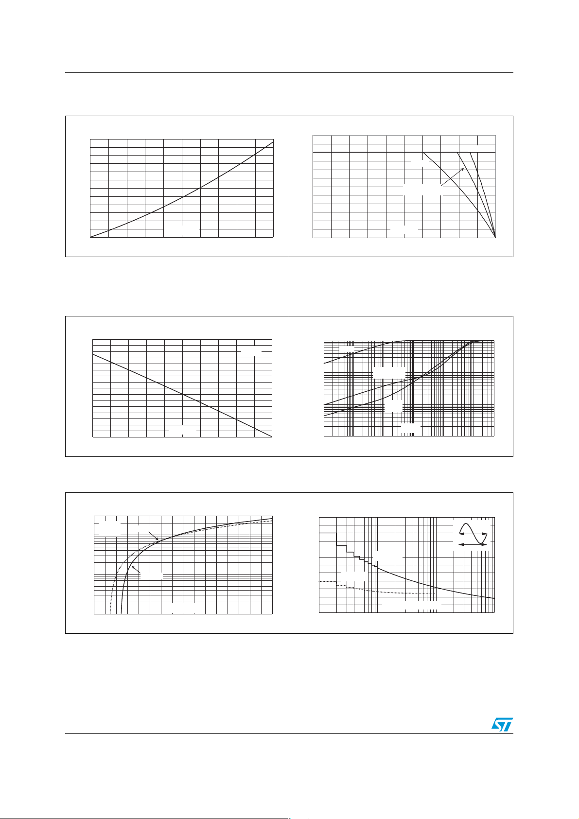
Figure 1. Maximum power dissipation versus
RMS on-state current (full cycle)
P(W)
30
25
20
15
10
5
0
0 5 10 15 20 25
I (A)
T(RMS)
Figure 3. D2PAK RMS on-state current versus
ambient temperature (printed
circuit board FR4, copper
thickness: 35µm) (full cycle)
I (A)
T(RMS)
4.0
3.5
3.0
2.5
2.0
1.5
1.0
0.5
0.0
0 25 50 75 100 125
T (°C)
amb
2
DPAK
(S=1cm )
2
Figure 2. RMS on-state current versus case
temperature (full cycle)
I (A)
T(RMS)
30
25
T (°C)
C
BTA24
BTB24 / T25xx /
BTA25 / BTA26
20
15
10
5
0
0 25 50 75 100 125
BTB26
Figure 4. Relative variation of thermal
impedance versus pulse
duration
K=[Z /R
1E+0
1E-1
1E-2
1E-3
1E-3 1E-2 1E-1 1E+0 1E+1 1E+2 5E+2
th th
Z
th(j-c)
]
Z
th(j-a)
BTA / BTB24 /T25
Z
th(j-a)
BTA26
t (s)
p
Figure 5. On-state characteristics
(maximum values)
I (A)
TM
300
T max.
j
V = 0.85V
to
R = 16 m
d
100
10
1
0.5 1.0 1.5 2.0 2.5 3.0 3.5 4.0 4.5
4/12
T=jT max.
j
Ω
T = 25°Cj.
V (V)
TM
Figure 6. Surge peak on-state current
versus number of cycles
I (A)
TSM
300
250
200
150
100
50
0
Repetitive
T =75°C
1 10 100 1000
Non repetitive
T initial=25°C
j
C
Number of cycles
t=20ms
One cycle
 Loading...