

Features
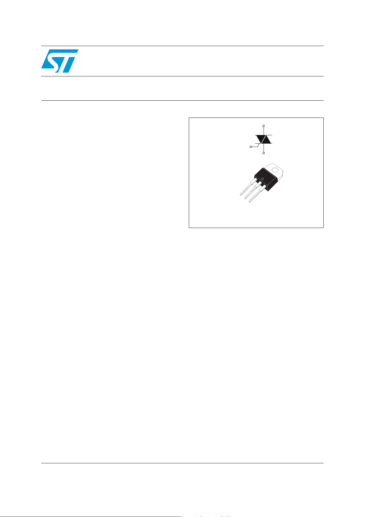
TO-220AB Insulated
A2
A1
G
G
A2
A1
BTA20
20 A Snubberless™ Triacs
Datasheet production data
■ I
■ V
■ I
= 20 A
T(RMS)
DRM
GT (Q1)
, V
= 600 and 700 V
RRM
(max) = 35 and 50 mA
Description
The BTA20 Triacs use high performance glass
passivated chip technology. The Snubberless
concept offers suppression of the RC network and
is suitable for applications such as phase control
and static switching on inductive or resistive load.
Thanks to their clip assembly technique, the
BTA20 Triacs provide a superior performance in
surge current handling capabilities.
By using an internal ceramic pad, the BTA series
provides voltage insulated tab (rated at
2500 V rms) complying with UL standards (File
ref.: E81734).
TM: Snubberless is a trademark of STMicroelectronics.
July 2012 Doc ID 2932 Rev 3 1/8
This is information on a product in full production.
www.st.com
8
Characteristics BTA20
1 Characteristics
Table 1. Absolute maximum ratings
Symbol Parameter Value Unit
I
T(RMS)
I
TSM
dI/dt
V
DSM
V
RSM
I
GM
V
P
G(AV)
T
Table 2. Electrical characteristics (Tj = 25 °C, unless otherwise specified)
On-state rms current (full sine wave) Tc = 70 °C 20 A
Non repetitive surge peak on-state
current (full cycle, Tj initial = 25°C)
²
tI²t Value for fusing tp = 10 ms 200 A²s
I
Critical rate of rise of on-state current
= 2 x IGT, tr 100 ns
I
G
,
Non repetitive peak off-state voltage tp = 10 ms Tj = 25 °C
F = 50 Hz t = 10 ms 210
F = 60 Hz t = 8.3 ms 200
Repetitive
F = 50 Hz
T
= 125 °C
j
50
Non repetitive 100
V
DSM/VRSM
100
Peak gate current tp = 20 µs Tj = 125 °C 4 A
Peak positive gate voltage tp = 20 µs 16 V
GM
Average gate power dissipation Tj = 125 °C 1 W
Storage junction temperature range - 40 to + 150
stg
Operating junction temperature range - 40 to + 125
T
j
BTA20
Symbol Test conditions Quadrant
BW CW
+
A
A/µs
V
°C
Unit
(1)
IGT
VD = 12 V, RL = 33
V
GT
V
GD
I
H
I
dV/dt
(dV/dt)c
1. Minimum IGT is guaranteed at 5% of IGT max.
2. For both polarities of A2 referenced to A1.
VD = V
DRM, RL
(2)
IT = 500 mA, gate open Max. 75 50 mA
IG = 1.2 I
L
(2)
VD = 67% V
(2)
(dI/dt)c = 20 A/ms Tj = 125 °C
= 3.3 kTj = 125 °C ALL Min. 0.2 V
GT
gate open Tj = 125 °C
DRM,
2/8 Doc ID 2932 Rev 3
ALL
Min. 2 1
Max. 50 35
ALL Max. 1.5 V
I - III
50 -
Ty p.
I - II - III Max. - 80
Ty p. 7 5 0 5 0 0
Min. 500 250
Typ. 36 22
Min. 18 11
mA
mAII 90 -
V/µs
V/µs
BTA20 Characteristics
0 5 10 15 20
0
10
5
15
20
25
30
P(W)
I (A)
T(RMS)
180°
α
α
α = 180°
α = 120°
α = 90°
α = 30°
α = 60°
0 20 40 60 80 100 120
P(W)
125
85
75
65
95
115
105
T (°C)
case
R = 1.5°C/W
th
R = 1°C/W
th
R = 0.5°C/W
th
R = 0°C/W
th
T (°C)
amb
0
10
5
15
20
25
30
(Tamb andTcase) for different thermal
resistances heatsink + contact
0 10 20 30 40 50 60 70 80 90 100 110 120 130
0
5
10
15
25
20
I (A)
T(RMS)
T (°C)
C
α = 180°
t (s)
p
1.E-3 1.E-2 1.E-1 1.E+0 1.E+1 1.E+2 5.E+2
0.01
0.1
1
K=[Z /R
th th
]
Z
th(j-c)
Z
th(j-a)
Table 3. Static characteristics
Symbol Parameter Value Unit
(1)
V
TM
I
DRM
I
RRM
ITM = 28 A, tp = 380 µs
V
= V
DRM
RRM
1. For both polarities of A2 referenced to A1.
Table 4. Thermal resistances
= 125 °C
T
j
Tj = 125 °C
Tj = 125 °C
Max. 1.70 V
10 µA
Max.
3mA
Symbol Parameter Value Unit
R
Junction to case for AC 2.1
th(j-c)
Junction to case for DC 2.8
th(j-c)
R
th(j-a)
Junction to ambient 60
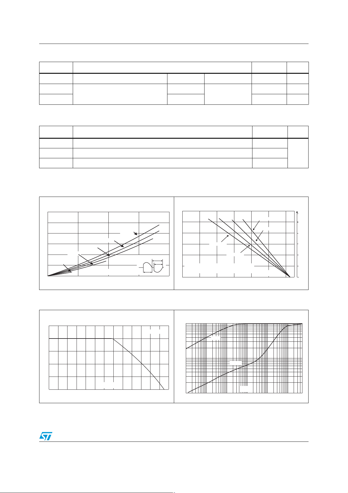
Figure 1. Maximum power dissipation versus
on-state rms current (full cycle)
Figure 2. Correlation between maximum rms
power dissipation and maximum
°C/WR
allowable temperatures
Figure 3. On-state rms current versus case
temperature (full cycle)
Figure 4. Relative variation of thermal
impedance versus pulse duration
Doc ID 2932 Rev 3 3/8

Characteristics BTA20
12345
1
10
100
1000
I (A)
TM
V (V)
TM
T = 25°Cj.
T=jT max.
j
T max.
V = 1.04V
R = 20 m
j
t0
d
Ω
1 10 100 1000
100
1000
I (A)
TSM
Number of cycles
t=20ms
One cycle
Non repetitive
T initial=25°C
j
0.01 0.10 1.00 10.00
100
1000
I (A), I t (A s)
TSM
22
t (ms)
p
T initial=25°C
j
I
TSM
I t
2
pulse width t 10 ms≤
-40 -30 -20 -10 0 20 3010 40 50 60 70 80 90 110100 130120
0.0
0.5
1.0
1.5
2.0
2.5
I,I,I[T] /
GT H L j
I ,I ,I [T =25°C]
GT H L j
T (°C)
j
I
GT
IH& I
L
Figure 5. On-state characteristics
(maximum values)
Figure 7. Non repetitive surge peak on-state
current for a sinusoidal pulse and
corresponding value of I
2
t
Figure 6. Non repetitive surge peak on-state
current versus number of cycles
Figure 8. Relative variation of gate trigger
current and holding current versus
junction temperature
4/8 Doc ID 2932 Rev 3

BTA20 Ordering information scheme
BT A 20 - 600 BW RG
Triac series
Insulation
Current
Voltage
Sensitivity and type
Packing mode
A = insulated
20 = 20A
600 = 600V
700 = 700V
BW = 50mA (max.)
CW = 35mA (max)
RG = Tube
2 Ordering information scheme
Figure 9. Ordering information scheme
Table 5. Product selector
Voltag e
Order code
600 V 700 V
Sensitivity Type Package
BTA20-600CWRG X 35 mA
BTA20-700CWRG X 35 mA
Snubberless TO-220AB Ins.BTA20-700BWRG X 50 mA
Doc ID 2932 Rev 3 5/8

Package information BTA20
C
b2
c2
F
Ø I
L
A
a1
a2
B
e
b1
I4
l3
l2
c1
M
3 Package information
● Epoxy meets UL94, V0
● Lead-free package
In order to meet environmental requirements, ST offers these devices in different grades of
ECOPACK
specifications, grade definitions and product status are available at: www.st.com
ECOPACK
Table 6. TO-220AB dimensions
®
packages, depending on their level of environmental compliance. ECOPACK®
®
is an ST trademark.
.
Dimensions
Ref.
Millimeters Inches
Min. Typ. Max. Min. Typ. Max.
A 15.20 15.90 0.598 0.625
a1 3.75 0.147
a2 13.00 14.00 0.511 0.551
B 10.00 10.40 0.393 0.409
b1 0.61 0.88 0.024 0.034
b2 1.23 1.32 0.048 0.051
C 4.40 4.60 0.173 0.181
c1 0.49 0.70 0.019 0.027
c2 2.40 2.72 0.094 0.107
e 2.40 2.70 0.094 0.106
F 6.20 6.60 0.244 0.259
ØI 3.75 3.85 0.147 0.151
I4 15.80 16.40 16.80 0.622 0.646 0.661
L 2.65 2.95 0.104 0.116
l2 1.14 1.70 0.044 0.066
l3 1.14 1.70 0.044 0.066
M2.60 0.102
6/8 Doc ID 2932 Rev 3

BTA20 Ordering information
4 Ordering information
Table 7. Ordering information
Ordering type Marking Package Weight Base qty Delivery mode
BTA20-600CWRG BTA20-600CW
TO-220AB Ins. 2.3 g 50 TubeBTA20-700BWRG BTA20-700BW
BTA20-700CWRG BTA20-700CW
5 Revision history
Table 8. Document revision history
Date Revision Changes
Sep-2001 1A Initial release.
08-Feb-2006 2 TO-220AB Ins. delivery mode changed from bulk to tube.
09-Jul-2012 3 Updated dI/dt repetitive value in Table 1.
Doc ID 2932 Rev 3 7/8

BTA20
Please Read Carefully:
Information in this document is provided solely in connection with ST products. STMicroelectronics NV and its subsidiaries (“ST”) reserve the
right to make changes, corrections, modifications or improvements, to this document, and the products and services described herein at any
time, without notice.
All ST products are sold pursuant to ST’s terms and conditions of sale.
Purchasers are solely responsible for the choice, selection and use of the ST products and services described herein, and ST assumes no
liability whatsoever relating to the choice, selection or use of the ST products and services described herein.
No license, express or implied, by estoppel or otherwise, to any intellectual property rights is granted under this document. If any part of this
document refers to any third party products or services it shall not be deemed a license grant by ST for the use of such third party products
or services, or any intellectual property contained therein or considered as a warranty covering the use in any manner whatsoever of such
third party products or services or any intellectual property contained therein.
UNLESS OTHERWISE SET FORTH IN ST’S TERMS AND CONDITIONS OF SALE ST DISCLAIMS ANY EXPRESS OR IMPLIED
WARRANTY WITH RESPECT TO THE USE AND/OR SALE OF ST PRODUCTS INCLUDING WITHOUT LIMITATION IMPLIED
WARRANTIES OF MERCHANTABILITY, FITNESS FOR A PARTICULAR PURPOSE (AND THEIR EQUIVALENTS UNDER THE LAWS
OF ANY JURISDICTION), OR INFRINGEMENT OF ANY PATENT, COPYRIGHT OR OTHER INTELLECTUAL PROPERTY RIGHT.
UNLESS EXPRESSLY APPROVED IN WRITING BY TWO AUTHORIZED ST REPRESENTATIVES, ST PRODUCTS ARE NOT
RECOMMENDED, AUTHORIZED OR WARRANTED FOR USE IN MILITARY, AIR CRAFT, SPACE, LIFE SAVING, OR LIFE SUSTAINING
APPLICATIONS, NOR IN PRODUCTS OR SYSTEMS WHERE FAILURE OR MALFUNCTION MAY RESULT IN PERSONAL INJURY,
DEATH, OR SEVERE PROPERTY OR ENVIRONMENTAL DAMAGE. ST PRODUCTS WHICH ARE NOT SPECIFIED AS "AUTOMOTIVE
GRADE" MAY ONLY BE USED IN AUTOMOTIVE APPLICATIONS AT USER’S OWN RISK.
Resale of ST products with provisions different from the statements and/or technical features set forth in this document shall immediately void
any warranty granted by ST for the ST product or service described herein and shall not create or extend in any manner whatsoever, any
liability of ST.
ST and the ST logo are trademarks or registered trademarks of ST in various countries.
Information in this document supersedes and replaces all information previously supplied.
The ST logo is a registered trademark of STMicroelectronics. All other names are the property of their respective owners.
© 2012 STMicroelectronics - All rights reserved
STMicroelectronics group of companies
Australia - Belgium - Brazil - Canada - China - Czech Republic - Finland - France - Germany - Hong Kong - India - Israel - Italy - Japan -
Malaysia - Malta - Morocco - Philippines - Singapore - Spain - Sweden - Switzerland - United Kingdom - United States of America
www.st.com
8/8 Doc ID 2932 Rev 3
 Loading...