

ST BTA16B, BTB16B User Manual
查询BTA16-400B供应商
FEATURES
.HIGHSURGECURRENT CAPABILITY
.COMMUTATION : (dV/dt)c>10V/µs
.BTA Family :
INSULATINGVOLTAGE= 2500V
(ULRECOGNIZED: E81734)
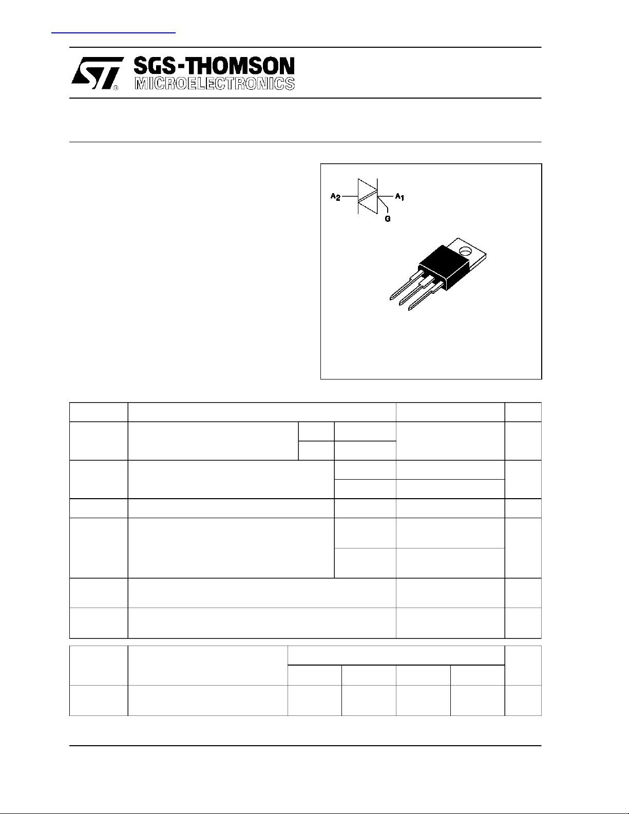
BTA16 B
BTB16 B
STANDARDTRIACS
(RMS)
DESCRIPTION
The BTA/BTB16 B triac family are high performance glass passivated PNPN devices.
These parts are suitables for general purpose applications where high surge current capability is required. Application such as phase control and
static switching on inductive or resistive load.
ABSOLUTE RATINGS (limitingvalues)
Symbol Parameter Value Unit
I
T(RMS)
I
TSM
I2tI
dI/dt Critical rate of rise of on-state current
RMS on-state current
(360° conduction angle)
Non repetitive surge peak on-state current
( Tj initial = 25°C)
2
t value tp = 10 ms 128 A2s
Gate supply : IG= 500mA diG/dt = 1A/µs
BTA Tc = 80 °C16 A
BTB Tc = 90 °C
tp = 8.3 ms 170 A
tp = 10 ms 160
Repetitive
F = 50 Hz
Repetitive
Non
A1
A2
G
TO220AB
(Plastic)
10 A/µs
50
Tstg
Tj
Tl Maximum lead temperature for soldering during 10 s at 4.5 mm
Symbol Parameter BTA / BTB16-... B Unit
V
DRM
V
RRM
March 1995
Storage and operating junction temperature range - 40 to + 150
- 40 to + 125
260 °C
from case
400 600 700 800
Repetitive peak off-state voltage
Tj = 125 °C
400 600 700 800 V
°C
°C
1/5
BTA16 B / BTB16 B
THERMAL RESISTANCES
Symbol Parameter Value Unit
Rth (j-a) Junction to ambient 60 °C/W
Rth (j-c) DC Junction to case for DC BTA 2.9 °C/W
BTB 2.3
Rth (j-c) AC Junction to case for 360° conduction angle
( F= 50 Hz)
BTA 2.2 °C/W
BTB 1.75
GATECHARACTERISTICS (maximum values)
P
=1W PGM= 10W (tp = 20 µs) IGM=4A(tp=20µs) VGM= 16V (tp = 20 µs).
G (AV)
ELECTRICAL CHARACTERISTICS
Symbol Test Conditions Quadrant Suffix Unit
B
I
GT
V
GT
V
GD
tgt VD=V
I
L
IH*I
VTM*ITM= 22.5A tp= 380µs Tj=25°C MAX 1.6 V
VD=12V (DC) RL=33Ω Tj=25°C I-II-III MAX 50 mA
IV MAX 100
VD=12V (DC) RL=33Ω Tj=25°C I-II-III-IV MAX 1.5 V
VD=V
DRMRL
DRMIG
dIG/dt = 3A/µs
IG=1.2 I
= 500mA gate open Tj=25°C MAX 50 mA
T
=3.3kΩ Tj=125°C I-II-III-IV MIN 0.2 V
= 500mA
GT
Tj=25°C I-II-III-IV TYP 2 µs
Tj=25°C I-III-IV TYP 40 mA
II 70
I
DRM
I
RRM
dV/dt * Linear slope up to VD=67%V
(dV/dt)c * (dI/dt)c = 7A/ms Tj=125°C MIN 10 V/µs
* For either polarity of electrode A2voltage with reference to electrode A1.
2/5
V
DRM
V
RRM
gate open
Rated
Rated
DRM
Tj=25°C MAX 0.01 mA
Tj=125°C MAX 2
Tj=125°C MIN 250 V/µs
 Loading...