

查询BTA10 GP供应商
FEATURES
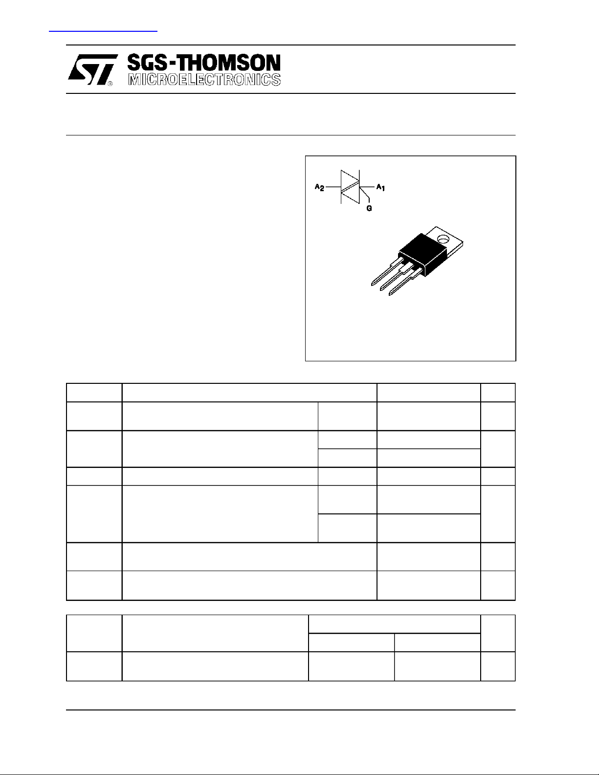
BTA10 GP
TRIACS
.LOWI
.HIGHSURGECURRENT : I
.I
GT
.INSULATINGVOLTAGE= 2500V
(ULRECOGNIZED: E81734)
DESCRIPTION
The BTA10 GP’s use high performance,glass passivated chips.
The insulated TO220AB package, the high surge
current and low holding current make this family
well adapted to LIGHT DIMMER applications.
ABSOLUTE RATINGS (limitingvalues)
Symbol Parameter Value Unit
I
T(RMS)
I
= 13mAmax
H
=120A
TSM
SPECIFIEDINFOURQUADRANTS
(RMS)
RMS on-state current
(360° conduction angle)
TSM
I2tI
Non repetitive surge peak on-state current
( Tj initial = 25°C)
2
t value tp = 10 ms 72 A2s
A1
A2
G
TO220AB
(Plastic)
Tc = 90 °C10 A
tp = 8.3 ms 126 A
tp = 10 ms 120
dI/dt Critical rate of rise of on-state current
Gate supply : IG= 500mA diG/dt = 1A/µs
Tstg
Tj
Tl Maximum lead temperature for soldering during 10 s at 4.5 mm
Symbol Parameter BTA10- Unit
V
DRM
V
RRM
March 1995
Storage and operating junction temperature range - 40 to + 150
from case
Repetitive peak off-state voltage
Tj = 125 °C
Repetitive
F = 50 Hz
Non
Repetitive
400 GP 600 GP
400 600 V
10 A/µs
50
- 40 to + 125
260 °C
°C
°C
1/4
BTA10 GP
THERMAL RESISTANCES
Symbol Parameter Value Unit
Rth (j-a) Junction to ambient 60 °C/W
Rth (j-c) DC Junction to case for DC 4 °C/W
Rth (j-c) AC Junction to case for360° conduction angle
( F= 50 Hz)
3 °C/W
GATECHARACTERISTICS (maximumvalues)
P
G (AV)
=1W PGM= 10W (tp = 20 µs) IGM=4A(tp=20µs) VGM= 16V (tp = 20 µs).
ELECTRICAL CHARACTERISTICS
Symbol Test Conditions Quadrant Suffix Unit
GP
I
GT
V
GT
V
GD
tgt VD=V
I
L
VD=12V (DC) RL=33Ω Tj=25°C I-II-III MAX 50 mA
IV MAX 75
VD=12V (DC) RL=33Ω Tj=25°C I-II-III-IV MAX 1.5 V
VD=V
DRMRL
DRMIG
dIG/dt = 3A/µs
IG=1.2 I
=3.3kΩ Tj=110°C I-II-III-IV MIN 0.2 V
= 500mA
GT
Tj=25°C I-II-III-IV TYP 2 µs
Tj=25°C I-III-IV TYP 20 mA
II 40
IH*I
VTM*ITM= 14A tp= 380µs Tj=25°C MAX 1.5 V
I
DRM
I
RRM
dV/dt * Linear slope up to VD=67%V
(dV/dt)c * (dI/dt)c= 2.2A/ms Tj=110°C MIN 1 V/µs
* For either polarity of electrode A2voltage with reference to electrode A1.
2/4
= 100mA gate open Tj=25°C MAX 13 mA
T
V
V
gate open
DRM
RRM
Rated
Rated
DRM
Tj=25°C MAX 0.01 mA
Tj=110°C MAX 0.5
Tj=110°C MIN 30 V/µs
TYP 100
TYP 10
 Loading...