

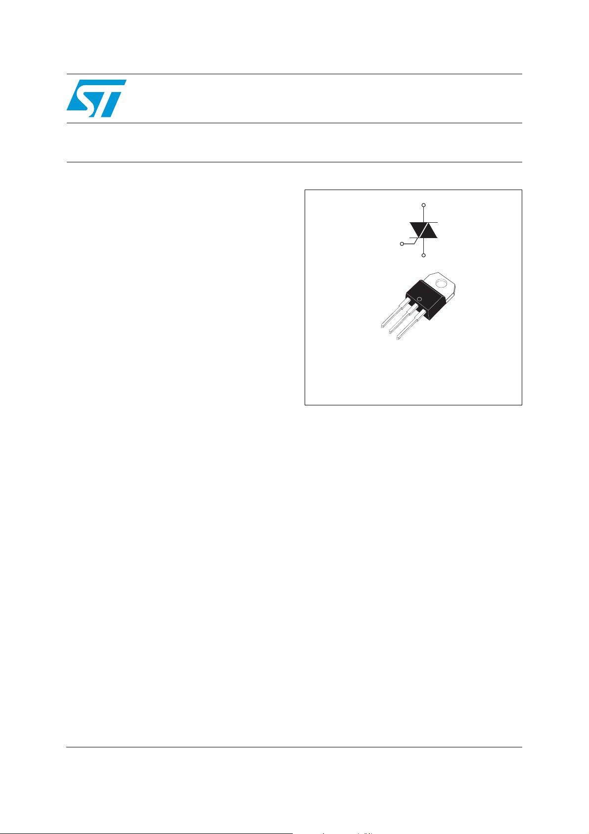
BTA10-600GP
10 A Triac
Features
■ Low I
■ High surge current:
■ I
■ Insulating voltage:
:
H
– 13 mA max
–I
GT
– 2500 V
= 120 A
TSM
specified in four quadrants
(UL Recognized: E81734)
(RMS)
Description
The BTA10-600GP uses high performance, glass
passivated chips.
The insulated TO-220AB package, the high surge
current and low holding current make this product
well adapted to CFL and LED dimmer
applications.
A2
G
A1
A1
A2
G
TO-220AB
September 2011 Doc ID 022222 Rev 1 1/7
www.st.com
7
Characteristics BTA10-600GP
1 Characteristics
Table 1. Absolute ratings (limiting values)
Symbol Parameter Value Unit
V
DRM
V
RRM
I
T(RMS)
I
TSM
2
I
dI/dt
T
stg
T
Table 2. Electrical characteristics
Repetitive peak off-state voltage Tj = 125° C 600 V
RMS on-state current (360° conduction angle) Tc = 90° C 10 A
Non repetitive surge peak on-state current
initial = 25° C)
(T
j
tI
²
t Value for fusing tp = 10 ms 72 A2s
tp = 8.3 ms 126
= 10 ms 120
t
p
Repetitive
Critical rate of rise of on-state current
= 500 mA diG/dt = 1 A/µs
I
G
Storage junction temperature range
Operating junction temperature range
j
F = 50 Hz
Non repetitive 50
-40 to +150
-40 to +125
10
Symbol Test conditions Quadrant Value Unit
(1)
I
GT
V
GT
V
GD
t
gt
I
L
(1)
I
H
(1)
V
TM
I
DRM
I
RRM
dV/dt
(dV/dt)c
VD = 12 V (DC) RL = 33 Ω Tj = 25° C
VD = 12 V (DC) RL = 33 Ω Tj = 25° C I - II - III - IV MAX 1.5 V
VD = V
VD = V
IG = 1.2 I
RL = 3.3 kΩ Tj = 110° C I - II - III - IV MIN 0.2 V
DRM
DRM IG
= 500 mA dIG/dt = 3 A/µs Tj = 25° C I - II - III - IV TYP 2 µs
GT
Tj = 25° C
IT = 100 mA gate open Tj = 25° C MAX 13 mA
ITM = 14 A tp = 380 µs Tj = 25° C MAX 1.5 V
Tj = 25° C MAX 0.01
V
= V
DRM
Linear slope up to VD = 67% V
(1)
gate open
(1)
(dI/dt)c = 2.2 A/ms Tj = 110° C
RRM
DRM
= 110° C MAX 0.5
T
j
= 110° C
T
j
I - II- III MAX 25
IV MAX 100
I - II - III
TYP
IV 40
MIN 30
TYP 100
MIN 1
20
TYP 10
A
A/µs
° C
mA
mA
mA
V/µs
V/µs
1. For either polarity of electrode A2 voltage with reference to electrode A1.
2/7 Doc ID 022222 Rev 1
BTA10-600GP Characteristics
Table 3. Gate characteristics (maximum values)
Symbol Parameter Value Unit
P
G(AV)
P
GM
I
GM
V
GM
Table 4. Thermal resistances
Average gate power dissipation 1 W
Peak gate power dissipation tp = 20 µs 10 W
Peak gate current tp = 20 µs 4 A
Peak positive gate voltage tp = 20 µs 16 V
Symbol Parameter Value Unit
R
th(j-a)
th(j-c)
R
th(j-c)
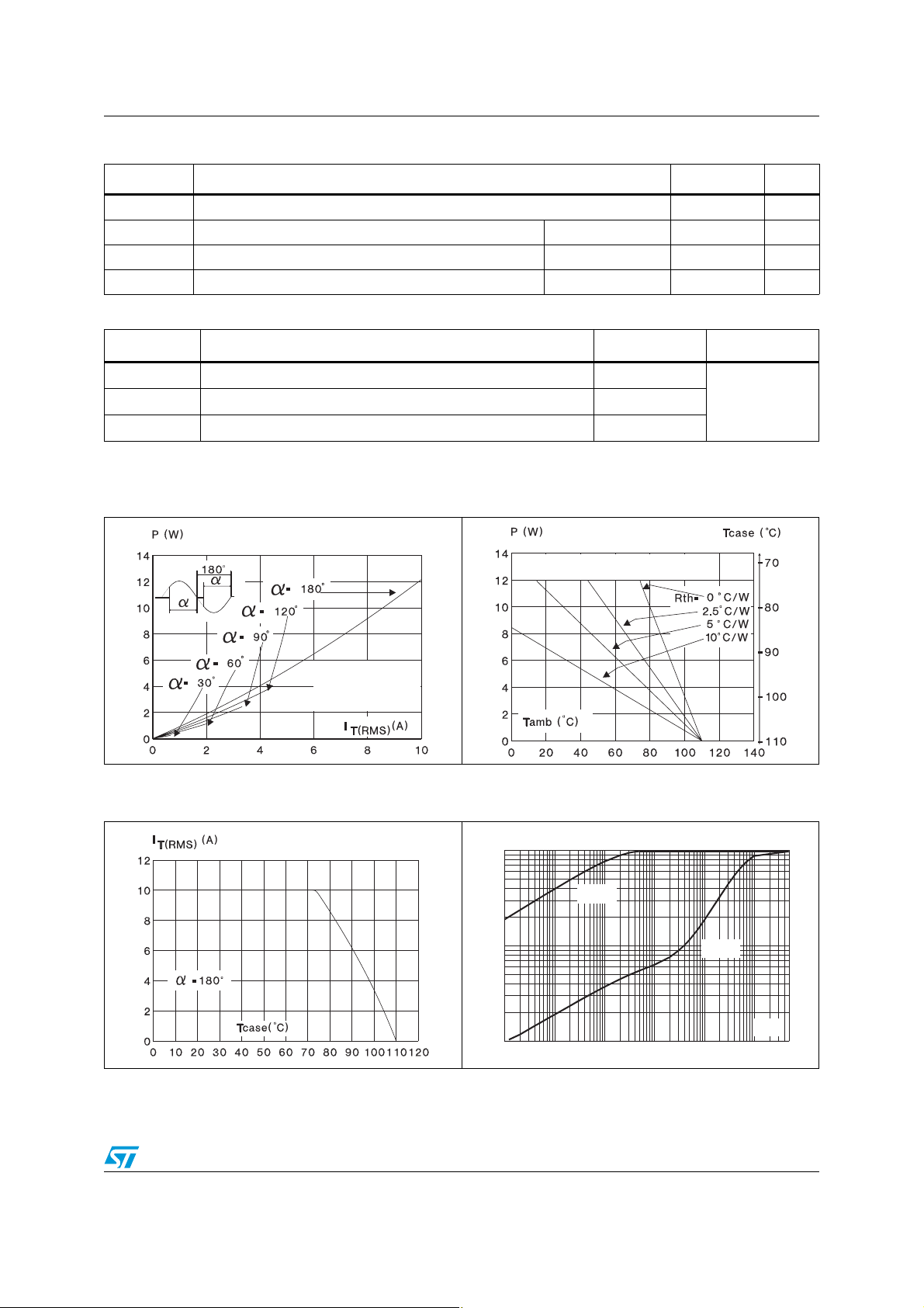
Figure 1. Maximum rms power dissipation
Junction to ambient 60
DC Junction to case for DC 4
AC Junction to case for 360° conduction angle (F = 50 Hz) 3
Figure 2. Maximum rms power dissipation
versus rms on-state current
and maximum allowable
temperatures (T
For different thermal resistances
heatsink + contact
amb
and T
° C/WR
case
)
F = 50 Hz, curves
are cut off by
(dI/dt)climitation
Figure 3. On-state rms current versus case
temperature
Figure 4. Relative variation of thermal
impedance versus pulse duration
Zth/Rth
1
Zth(j-c)
0.1
0.01
1E-3 1E-2 1E-1 1E+0 1E+1 1E+2 5E+2
Zth(j-a)
tp(s)
Doc ID 022222 Rev 1 3/7
 Loading...