

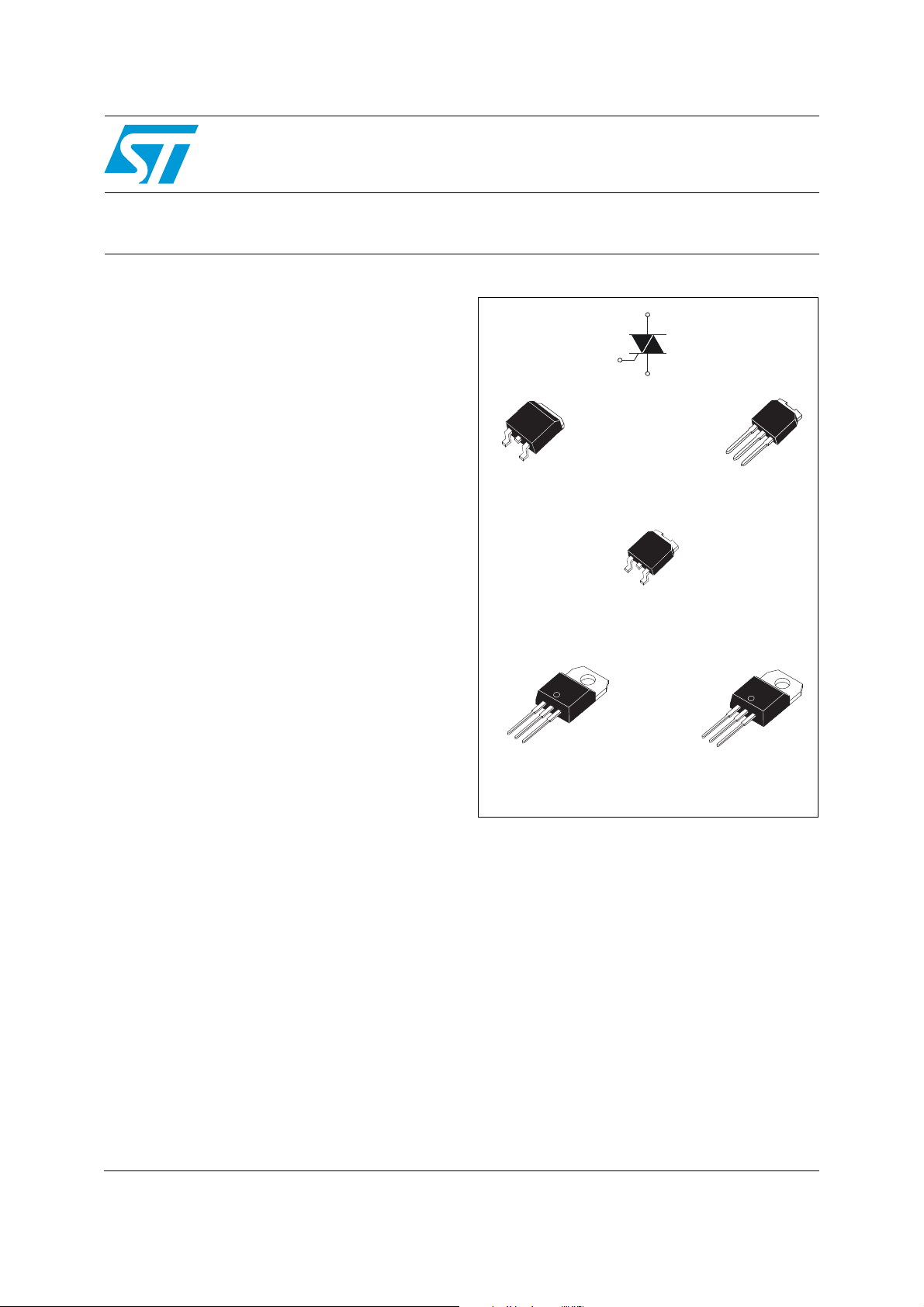
BTA08, BTB08
T810, T835
Snubberless™, logic level and standard 8 A Triacs
Features
■ On-state rms current, I
■ Repetitive peak off-state voltage, V
600 to 800 V
■ Triggering gate current, I
T(RMS)
GT (Q1)
8 A
DRM/VRRM
5 to 50 mA
Description
Available either in through-hole or surface-mount
packages, the BTA08, BTB08 and T8 triac series
is suitable for general purpose AC switching. They
can be used as an ON/OFF function in
applications such as static relays, heating
regulation, induction motor starting circuits... or
for phase control operation in light dimmers,
motor speed controllers,...
The snubberless versions (BTA/BTB...W and T8
series) are specially recommended for use on
inductive loads, thanks to their high commutation
performances.
Logic level versions are designed to interface
directly with low power drivers such as
microcontrollers.
By using an internal ceramic pad, the BTA series
provides voltage insulated tab (rated at 2500
V
) complying with UL standards (file ref.:
RMS
E81734).
A2
A2
A1
A2
G
D2PAK
(T8-G)
G
A1
A2
A1
A2
G
IPAK
(T8-H)
A2
A1
A2
G
DPAK
(T8-B)
A2
A1
A2
G
TO-220AB Insulated
(BTA08)
A1
A2
G
TO-220AB
(BTB08)
March 2010 Doc ID 7472 Rev 7 1/12
www.st.com
12
Characteristics BTA08, BTB08 and T8 Series
1 Characteristics
Table 1. Absolute maximum ratings
Symbol Parameter Value Unit
I
T(RMS)
On-state rms current (full sine wave)
IPAK/D2PAK/DPAK/
TO-220AB
= 110 °C
T
c
8A
TO-220AB Ins. Tc = 100 °C
I
dI/dt
Non repetitive surge peak on-state current
TSM
(full cycle, T
²
tI²t value for fusing tp = 10 ms 36 A²s
I
Critical rate of rise of on-state current I
x I
GT
,
initial = 25 °C)
j
G
F = 50 Hz t = 20 ms 80
F = 60 Hz t = 16.7 ms 84
= 2
F = 120 Hz Tj = 125 °C 50 A/µs
tr ≤ 100 ns
I
Peak gate current tp = 20 µs Tj = 125 °C 4 A
GM
P
T
Table 2. Electrical characteristics (Tj = 25 °C, unless otherwise specified)
Average gate power dissipation Tj = 125 °C 1 W
G(AV)
Storage junction temperature range
stg
T
Operating junction temperature range
j
- 40 to + 150
- 40 to + 125
Snubberless and logic level (3 quadrants)
T8 BTA08 / BTB08
Symbol Test conditions Quadrant
(1)
I
GT
V
V
I
H
VD = 12 V RL = 30 Ω
GT
VD = V
GD
= 125 °C
T
j
(2)
IT = 100 mA MAX. 15 35 10 15 35 50 mA
DRM RL
= 3.3 kΩ
I - II - III MAX. 10 35 5 10 35 50 mA
I - II - III MAX. 1.3 V
I - II - III MIN. 0.2 V
I - III
I
IG = 1.2 I
L
GT
II 30 60 15 30 60 80
T810 T835 TW SW CW BW
25 50 10 25 50 70
MAX.
Unit
A
°C
mA
dV/dt
(dI/dt)c
(2)
VD = 67 %V
(2)
Tj = 125 °C
(dV/dt)c = 0.1 V/µs Tj = 125 °C
Without snubber T
gate open
DRM
MIN. 40 400 20 40 400 1000 V/µs
5.4 - 3.5 5.4 - -
= 125 °C 2.8 - 1.5 2.98 - -
j
= 125 °C - 4.5 - - 4.5 7
j
MIN.
2/12 Doc ID 7472 Rev 7
A/ms(dV/dt)c = 10 V/µs T
BTA08, BTB08 and T8 Series Characteristics
Table 3. Standard (4 quadrants)
BTA08 / BTB08
Symbol Test conditions Quadrant
Unit
CB
(1)
I
GT
V
V
I
H
dV/dt
(dV/dt)c
Table 4. Static characteristics
VD = 12 V, RL = 33 Ω
GT
VD = V
GD
(2)
IT = 500 mA MAX. 25 50 mA
I
IG = 1.2 I
L
(2)
VD = 67 %V
(dI/dt)c = 5.3 A/ms Tj = 125 °C MIN. 5 10 V/µs
(2)
, RL = 3.3 kΩ, Tj = 125 °C ALL MIN. 0.2 V
DRM
GT
gate open Tj = 125 °C MIN. 200 400 V/µs
DRM
I - II - III
IV
MAX.
ALL MAX. 1.3 V
I - III - IV
MAX.
II 80 100
25
50
50
100
40 50
Symbol Test conditions Value Unit
(1)
V
TM
V
R
I
DRM
I
RRM
1. minimum IGT is guaranted at 5% of IGT max.
2. for both polarities of A2 referenced to A1.
Table 5. Thermal resistance
ITM = 11 A, tp = 380 µs Tj = 25 °C MAX. 1.55 V
(2)
Threshold voltage Tj = 125 °C MAX. 0.85 V
t0
(2)
Dynamic resistance Tj = 125 °C MAX. 50 mΩ
d
Tj = 25 °C
V
DRM
= V
RRM
= 125 °C 1 mA
T
j
MAX.
5µA
mA
mA
Symbol Parameter Value Unit
2
PAK / DPAK / TO-220AB 1.6
°C/W
°C/W
R
R
Junction to case (AC)
th(j-c)
Junction to ambient
th(j-a)
S = 1 cm
S = 0.5 cm
IPAK / D
TO-220AB Insulated 2.5
²
D2PA K 4 5
²
DPAK 70
TO-220AB / TO-220AB Insulated 60
IPAK 100
S = Copper surface under tab.
Doc ID 7472 Rev 7 3/12
Characteristics BTA08, BTB08 and T8 Series
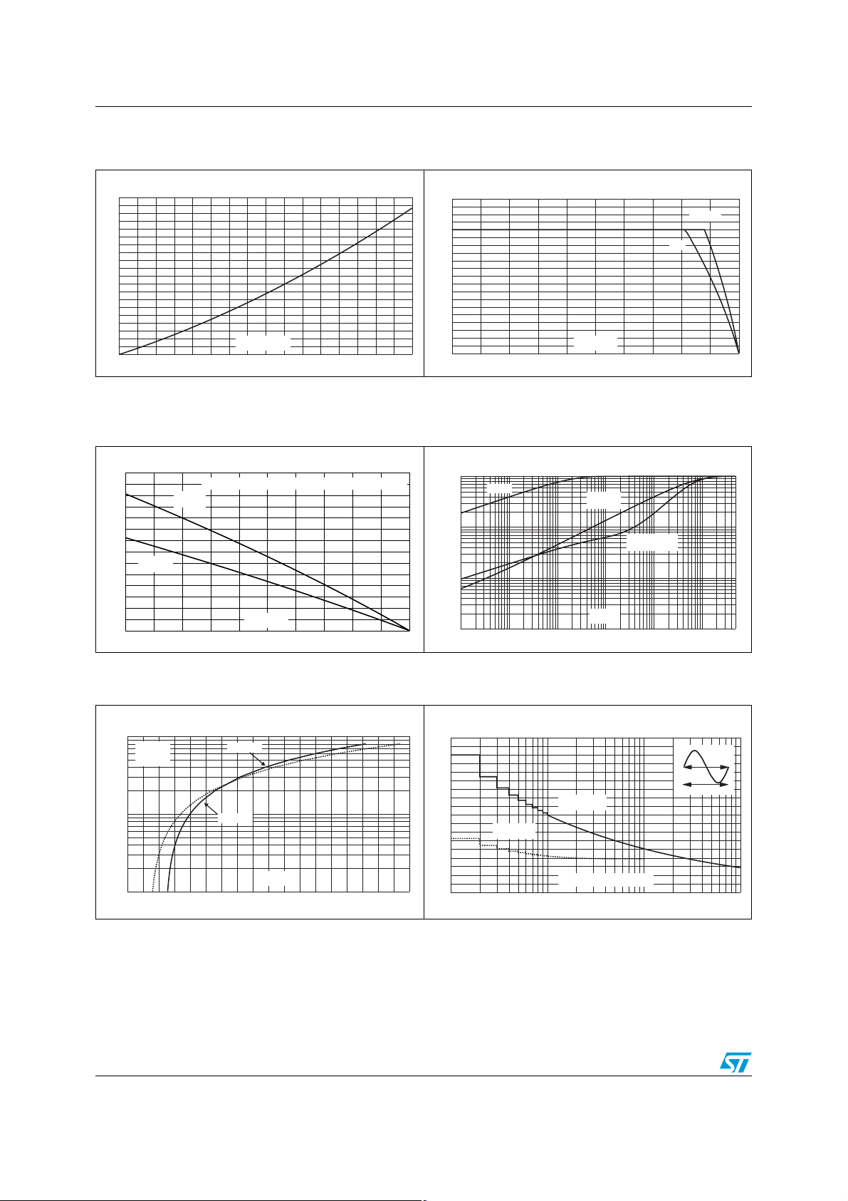
Figure 1. Maximum power dissipation versus
rms on-state current (full cycle)
P(W)
10
9
8
7
6
5
4
3
2
1
0
012345678
I (A)
T(RMS)
Figure 3. On-state rms current versus
ambient temperature (full cycle)
I (A)
T(RMS)
3.5
3.0
2.5
2.0
1.5
DPAK
(S=0.5CM )
1.0
0.5
0.0
0 25 50 75 100 125
printed circuit board FR4, copper thickness: 35 µm
2
DPAK
2
(S=1CM )
2
T (°C)
C
Figure 2. On-state rms current versus case
temperature (full cycle)
I (A)
T(RMS)
10
9
8
7
6
5
4
3
2
1
0
0 25 50 75 100 125
T (°C)
C
BTB / T8
BTA
Figure 4. Relative variation of thermal
impedance versus pulse
duration
K=[Z /R
1E+0
1E-1
1E-2
1E-3
1E-3 1E-2 1E-1 1E+0 1E+1 1E+2 5E+2
th th
Z
th(j-c)
]
DPAK/IPAK
Z
th(j-a)
2
TO-220AB/D PAK
Z
th(j-a)
t (s)
p
Figure 5. On-state characteristics
Figure 6. Surge peak on-state current
(maximum values)
I (A)
TM
100
T max.
j
V = 0.85V
to
Ω
R = 50 m
d
10
1
0.5 1.0 1.5 2.0 2.5 3.0 3.5 4.0 4.5 5.0
T=jT max.
T = 25°Cj.
j
V (V)
TM
4/12 Doc ID 7472 Rev 7
I (A)
TSM
90
80
70
60
50
40
30
20
10
0
1 10 100 1000
versus number of cycles
Non repetitive
T initial=25°C
j
Repetitive
T =110°C
C
Number of cycles
t=20ms
One cycle

BTA08, BTB08 and T8 Series Characteristics
Figure 7. Non-repetitive surge peak on-state
current for a sinusoidal
I (A), I t (A s)
1000
100
10
0.01 0.10 1.00 10.00
22
TSM
dI/dt limitation:
50A/µs
360°
α
pulse with width t < 10 ms and corresponding value of I t
p
T initial=25°C
j
I
TSM
2
I t
2
t (ms)
p
Figure 9. Relative variation of critical rate of
decrease of main current versus
(dV/dt)c (typical values)
(dI/dt)c [(dV/dt)c] / Specified (dI/dt)c
2.2
TW
2.0
1.8
1.6
1.4
1.2
1.0
0.8
0.6
0.4
0.2
0.0
0.1 1.0 10.0 100.0
Snubberless and Logic level types
T835/CW/BW
T810/SW
(dV/dt)c (V/µs)
Figure 8. Relative variation of gate trigger
current
I,I,I[T] /
GTHL j
2.5
2.0
1.5
1.0
0.5
0.0
-40 -20 0 20 40 60 80 100 120 140
IH& I
I
GT
L
I ,I ,I [T =25°C]
GTHL j
holding current and latching current
versus junction temperature (typical values)
T (°C)
j
Figure 10. Relative variation of critical rate of
decrease of main current versus
(dV/dt)c (typical values)
(dI/dt)c [(dV/dt)c] / Specified (dI/dt)c
2.0
1.8
1.6
1.4
1.2
1.0
0.8
0.6
0.4
0.1 1.0 10.0 100.0
C
B
(dV/dt)c (V/µs)
Standard types
Figure 11. Relative variation of critical rate of
decrease of main current versus
junction temperature
(dI/dt)c [T ] / pecified]
6
5
4
3
2
1
0
0 25 50 75 100 125
(dI/dt)c [T s
j
j
T (°C)
j
Doc ID 7472 Rev 7 5/12
Figure 12. DPAK and D2PAK thermal resistance
junction to ambient versus copper
surface under tab
R (°C/W)
th(j-a)
100
90
80
70
60
50
40
2
30
DPAK
20
10
0
0 4 8 1216202428323640
printed circuit board FR4, copper thickness: 35 µm
DPAK
S(cm²)

Package information BTA08, BTB08 and T8 Series
D
2 Package information
● Epoxy meets UL94, V0
● Lead-free packages
In order to meet environmental requirements, ST offers these devices in different grades of
ECOPACK
specifications, grade definitions and product status are available at: www.st.com
ECOPACK
Table 6. D
®
packages, depending on their level of environmental compliance. ECOPACK®
®
is an ST trademark.
2
PAK dimensions
.
Dimensions
Ref.
Millimeters Inches
Min. Typ. Max. Min. Typ. Max.
A 4.30 4.60 0.169 0.181
A
L2
E
C2
A1 2.49 2.69 0.098 0.106
A2 0.03 0.23 0.001 0.009
B 0.70 0.93 0.027 0.037
L
L3
G
B2
B
A1
2mm min.
FLAT ZONE
C
R
A2
V2
B2 1.25 1.40 0.048 0.055
C 0.45 0.60 0.017 0.024
C2 1.21 1.36 0.047 0.054
D 8.95 9.35 0.352 0.368
E 10.00 10.28 0.393 0.405
G 4.88 5.28 0.192 0.208
L 15.00 15.85 0.590 0.624
L2 1.27 1.40 0.050 0.055
L3 1.40 1.75 0.055 0.069
Figure 13. Footprint (dimensions in mm)
16.90
10.30
8.90
6/12 Doc ID 7472 Rev 7
R 0.40 0.016
V2 0° 8° 0° 8°
5.08
1.30
3.70

BTA08, BTB08 and T8 Series Package information
Table 7. DPAK dimensions
Dimensions
E
B2
L2
H
L4
B
G
0.60 MIN.
A1
A2
V2
A
C2
R
D
R
C
Figure 14. Footprint (dimensions in mm)
Ref.
Millimeters Inches
Min. Max. Min. Max.
A 2.20 2.40 0.086 0.094
A1 0.90 1.10 0.035 0.043
A2 0.03 0.23 0.001 0.009
B 0.64 0.90 0.025 0.035
B2 5.20 5.40 0.204 0.212
C 0.45 0.60 0.017 0.023
C2 0.48 0.60 0.018 0.023
D 6.00 6.20 0.236 0.244
E 6.40 6.60 0.251 0.259
G 4.40 4.60 0.173 0.181
H 9.35 10.10 0.368 0.397
L2 0.80 typ. 0.031 typ.
L4 0.60 1.00 0.023 0.039
V2 0° 8° 0° 8°
6.7
6.7 3 3
1.6
2.3
2.3
1.6
Doc ID 7472 Rev 7 7/12

Package information BTA08, BTB08 and T8 Series
Table 8. IPAK dimensions
Dimensions
Ref.
Millimeters Inches
Min. Typ. Max. Min. Typ. Max.
A 2.20 2.40 0.086 0.094
A1 0.90 1.10 0.035 0.043
A3 0.70 1.30 0.027 0.051
A
E
B2
L2
C2
B 0.64 0.90 0.025 0.035
B2 5.20 5.40 0.204 0.212
B3 0.95 0.037
B5 0.30 0.035
D
C 0.45 0.60 0.017 0.023
C2 0.48 0.60 0.019 0.023
H
L1
L
B3
B
V1
A1
D 6 6.20 0.236 0.244
E 6.40 6.60 0.252 0.260
e2.28 0.090
B5
e
G
C
A3
G 4.40 4.60 0.173 0.181
H 16.10 0.634
L 9 9.40 0.354 0.370
L1 0.8 1.20 0.031 0.047
L2 0.80 1 0.031 0.039
8/12 Doc ID 7472 Rev 7
V1 10° 10°

BTA08, BTB08 and T8 Series Package information
TO-220AB (NIns. and Ins. 20-up) dimensions
Dimensions
Ref.
Millimeters Inches
Min. Typ. Max. Min. Typ. Max.
A 15.20 15.90 0.598 0.625
a1 3.75 0.147
B
Ø I
C
b2
a2 13.00 14.00 0.511 0.551
B 10.00 10.40 0.393 0.409
L
A
I4
l3
a1
l2
e
a2
b1
F
b1 0.61 0.88 0.024 0.034
b2 1.23 1.32 0.048 0.051
C 4.40 4.60 0.173 0.181
c2
c1 0.49 0.70 0.019 0.027
c2 2.40 2.72 0.094 0.107
e 2.40 2.70 0.094 0.106
M
F 6.20 6.60 0.244 0.259
c1
ØI 3.75 3.85 0.147 0.151
I4 15.80 16.40 16.80 0.622 0.646 0.661
L 2.65 2.95 0.104 0.116
l2 1.14 1.70 0.044 0.066
l3 1.14 1.70 0.044 0.066
M2.60 0.102
Doc ID 7472 Rev 7 9/12

Ordering information BTA08, BTB08 and T8 Series
3 Ordering information
Figure 15. Ordering information scheme (BTA08 and BTB08 series)
BT A 08 - 600 BW (RG)
Triac series
Insulation
A = insulated
B = non insulated
Current
08 = 8A
Voltage
600 = 600V
800 = 800V
Sensitivity and type
B = 50mA Standard BW = 50mA Snubberless
C = 25mA Standard CW = 35mA
SW = 10mA Logic Level TW = 5mA Logic Level
Packing mode
RG = Tube
Figure 16. Ordering information scheme (T8 series)
Triac series
Current
8 = 8A
Sensitivity
10 = 10 mA
35 = 35 mA
Voltage
600 = 600 V
800 = 800 V
Packag e
B = DPAK
H = IPAK
2
G = D PAK
2
R = I PAK
Packing mode
Blanck = Tube
-TR = Tape and reel
Snubberless
T 8 10 - 600 B (-TR)
Table 9. Product Selector
Voltage (xxx)
Part Number
600 V 800 V
BTA/BTB08-xxxB X X 50 mA Standard TO-220AB
BTA/BTB08-xxxBW X X 50 mA Snubberless TO-220AB
BTA/BTB08-xxxC X X 25 mA Standard TO-220AB
BTA/BTB08-xxxCW X X 35 mA Snubberless TO-220AB
BTA/BTB08-xxxSW X X 10 mA Logic level TO-220AB
BTA/BTB08-xxxTW X X 5 mA Logic Level TO-220AB
T810-xxxG X X 10 mA Logic Level D
T810-xxxH X X 10 mA Logic Level IPAK
T835-xxxB X X 35 mA Snubberless DPAK
T835-xxxG X X 35 mA Snubberless D
T835-xxxH X X 35 mA Snubberless IPAK
BTB: non insulated TO-220AB package
10/12 Doc ID 7472 Rev 7
Sensitivity Type Package
2
PA K
2
PA K

BTA08, BTB08 and T8 Series Ordering information
4 Ordering information
Table 10. Ordering information
Order code Marking Package Weight Base qty Delivery mode
BTA/BTB08-xxxyzRG BTA/BTB08-xxxyz TO-220AB 2.3 g 50 Tube
T8yy-xxxG T8yyxx
T8yy-xxxG-TR T8yyxx 1000 Tape and reel
T8yy-xxxB T8yyxx
T8yy-xxxB-TR T8yyxx 2500 Tape and reel
T8yy-xxxH T8yyxx IPAK 0.4 g 75 Tube
xxx = voltage, yy = sensitivity, z = type
5 Revision history
Table 11. Document revision history
Date Revision Changes
Apr-2002 5A Last update.
13-Feb-2006 6
10-Mar-2010 7 Updated ECOPACK statement and Figure 16.
D2PAK 1.5 g
50 Tube
75 Tube
DPAK 0.3 g
TO-220AB delivery mode changed from bulk to tube.
ECOPACK statement added.
Doc ID 7472 Rev 7 11/12

BTA08, BTB08 and T8 Series
Please Read Carefully:
Information in this document is provided solely in connection with ST products. STMicroelectronics NV and its subsidiaries (“ST”) reserve the
right to make changes, corrections, modifications or improvements, to this document, and the products and services described herein at any
time, without notice.
All ST products are sold pursuant to ST’s terms and conditions of sale.
Purchasers are solely responsible for the choice, selection and use of the ST products and services described herein, and ST assumes no
liability whatsoever relating to the choice, selection or use of the ST products and services described herein.
No license, express or implied, by estoppel or otherwise, to any intellectual property rights is granted under this document. If any part of this
document refers to any third party products or services it shall not be deemed a license grant by ST for the use of such third party products
or services, or any intellectual property contained therein or considered as a warranty covering the use in any manner whatsoever of such
third party products or services or any intellectual property contained therein.
UNLESS OTHERWISE SET FORTH IN ST’S TERMS AND CONDITIONS OF SALE ST DISCLAIMS ANY EXPRESS OR IMPLIED
WARRANTY WITH RESPECT TO THE USE AND/OR SALE OF ST PRODUCTS INCLUDING WITHOUT LIMITATION IMPLIED
WARRANTIES OF MERCHANTABILITY, FITNESS FOR A PARTICULAR PURPOSE (AND THEIR EQUIVALENTS UNDER THE LAWS
OF ANY JURISDICTION), OR INFRINGEMENT OF ANY PATENT, COPYRIGHT OR OTHER INTELLECTUAL PROPERTY RIGHT.
UNLESS EXPRESSLY APPROVED IN WRITING BY AN AUTHORIZED ST REPRESENTATIVE, ST PRODUCTS ARE NOT
RECOMMENDED, AUTHORIZED OR WARRANTED FOR USE IN MILITARY, AIR CRAFT, SPACE, LIFE SAVING, OR LIFE SUSTAINING
APPLICATIONS, NOR IN PRODUCTS OR SYSTEMS WHERE FAILURE OR MALFUNCTION MAY RESULT IN PERSONAL INJURY,
DEATH, OR SEVERE PROPERTY OR ENVIRONMENTAL DAMAGE. ST PRODUCTS WHICH ARE NOT SPECIFIED AS "AUTOMOTIVE
GRADE" MAY ONLY BE USED IN AUTOMOTIVE APPLICATIONS AT USER’S OWN RISK.
Resale of ST products with provisions different from the statements and/or technical features set forth in this document shall immediately void
any warranty granted by ST for the ST product or service described herein and shall not create or extend in any manner whatsoever, any
liability of ST.
ST and the ST logo are trademarks or registered trademarks of ST in various countries.
Information in this document supersedes and replaces all information previously supplied.
The ST logo is a registered trademark of STMicroelectronics. All other names are the property of their respective owners.
© 2010 STMicroelectronics - All rights reserved
STMicroelectronics group of companies
Australia - Belgium - Brazil - Canada - China - Czech Republic - Finland - France - Germany - Hong Kong - India - Israel - Italy - Japan -
Malaysia - Malta - Morocco - Philippines - Singapore - Spain - Sweden - Switzerland - United Kingdom - United States of America
www.st.com
12/12 Doc ID 7472 Rev 7
 Loading...