BTA06T-600CWRG
6 A Snubberless™ Triac
Features
■ High static and dynamic commutation
■ BTA series is UL1557 certified (File ref.:
81734)
■ Package is RoHS (2002/95/EC) compliant
■ I
= 35 mA
GT
Applications
Specially designed for power tool applications, it
can also be used to drive loads like motor speed
controller, kitchen equipments such as electro
valves, light dimmers and similar.
Description
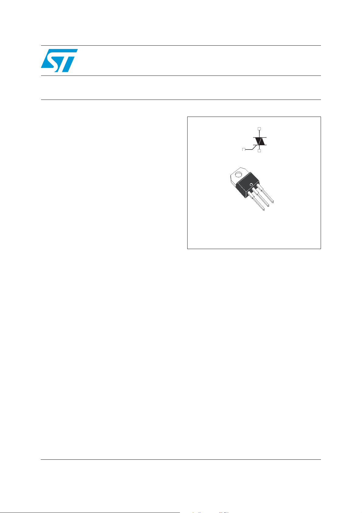
Available in through-hole package, the Triac
BTA06T-600CW is suitable for general purpose ac
switching.
Being a fully insulated package, the
BTA06T-600CW provides insulation rated at
2500 V rms.
A2
G
A1
G
A2
A1
TO-220AB insulated
BTA06T-600CW
TM: Snubberless is a trademark of STMicroelectronics
June 2010 Doc ID 17641 Rev 2 1/8
www.st.com
8

Characteristics BTA06T-600CWRG
1 Characteristics
Table 1. Absolute maximum ratings (limiting values)
Symbol Parameter Value Unit
I
T(RMS)
I
TSM
²
I
dI/dt
V
DSM/VRSM
I
GM
P
G(AV)
T
stg
T
Table 2. Electrical characteristics, Snubberless (3 quadrants)
On-state rms current (full sine wave) Tc = 100 °C 6 A
Non repetitive surge peak on-state current (full
cycle sine wave, Tj initial = 25 °C)
²
tI
t Value for fusing tp = 10 ms 13 A²s
Critical rate of rise of on-state current
I
= 2 x IGT, tr ≤ 100 ns
G
Non repetitive surge peak off-state voiltage tp = 10 ms Tj = 25 °C
F = 60 Hz t = 16.7 ms 47
F = 50 Hz t = 20 ms 45
F = 120 Hz Tj = 125 °C 50 A/µs
V
DRM/VRRM
Peak gate current tp = 20 µs Tj = 125 °C 4 A
Average gate power dissipation Tj = 125 °C 1 W
Storage junction temperature range
Operating junction temperature range
j
(T
= 25 °C, unless otherwise specified)
j
-40 to +150
-40 to +125
+ 100
Symbol Test conditions Quadrant Value Unit
(1)
I
GT
V
GT
V
GD
I
H
I
L
dV/dt
(dI/dt)c
1. Minimum IGT is guaranteed at 5% of IGT max.
2. For both polarities of A2 pin referenced to A1 pin
Table 3. Static electrical characteristics
VD = 12 V RL = 30 Ω I - II - III MAX 35 mA
VD = 12 V RL = 30 Ω I - II - III MAX 1.3 V
VD = V
(2)
IT = 100 mA MAX 35 mA
= 3.3 kΩ I - II - III MIN 0.2 V
DRM RL
I - III
IG = 1.2 x I
(2)
VD = 67% V
(2)
Without snubber, Tj = 125 °C MIN 8.0 A/ms
GT
, gate open, Tj = 125 °C MIN 750 V/µs
DRM
II 80
MAX
50
A
V
°C
mA
Symbol Test conditions Value Unit
(1)
I
V
TM
(1)
V
TO
(1)
R
D
I
DRM
I
RRM
1. For both polarities of A2 pin referenced to A1 pin
= 8.5 A, tp = 380 µs Tj = 25 °C MAX 1.6 V
TM
Threshold voltage Tj = 125 °C MAX 0.85 V
Dynamic resistance Tj = 125 °C MAX 80 mΩ
V
DRM
= V
RRM
Tj = 25 °C
MAX
T
= 125 °C 1 mA
j
5µA
2/8 Doc ID 17641 Rev 2

BTA06T-600CWRG Characteristics
/
Table 4. Thermal resistances
Symbol Parameter Value Unit
R
th(j-c)
R
th(j-a)
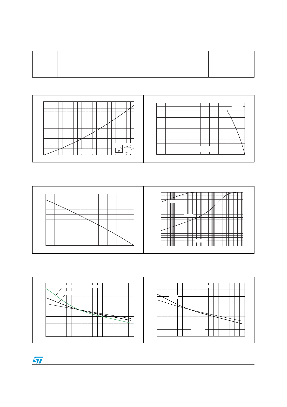
Figure 1. Maximum power dissipation versus
P(W)
8
7
6
5
4
3
2
1
0
0.0 0.5 1.0 1.5 2.0 2.5 3.0 3.5 4.0 4.5 5.0 5.5 6.0
Figure 3. On-state current (rms) versus
Junction to case (ac) 3.4
Junction to ambient 60
Figure 2. On-state current (rms) versus case
rms on-state current (full cycle)
α=180 °
I
(A)
T(RMS)
I
T(RMS)
7.0
6.0
5.0
4.0
3.0
2.0
180°
1.0
0.0
0 25 50 75 100 125
temperature (full cycle)
(A)
Figure 4. Relative variation of thermal
ambient temperature
impedance versus pulse duration
α=180°
TC(°C)
(free air convection)
K=[Z
Rth]
I
(A)
T(RMS)
2.5
2.0
1.5
α=180°
1.E+00
1.E-01
th
Zth(j-c)
Zth(j-a)
°C/W
1.0
0.5
0.0
0 25 50 75 100 125
T
(°C)
amb
Figure 5. Relative variation of gate trigger
current, and gate trigger voltage
versus junction temperature
IGT,VGT[Tj]/IGT,VGT[Tj=25 °C]
2.0
1.5
1.0
0.5
0.0
-40 -30 -20 -10 0 10 20 30 40 50 60 70 80 90 100 110 120 130
VGTQ1-Q2-Q3
IGTQ3
typical values
IGTQ1-Q2
Tj(°C)
1.E-02
tP(s)
1.E-03
1.E-03 1.E-02 1.E-01 1.E+00 1.E+01 1.E+02 1.E+03
Figure 6. Relative variation of holding
current and latching current versus
junction temperature
IH,IL[Tj]/IH,IL[Tj=25 °C]
2.0
1.5
1.0
0.5
0.0
-40 -30 -20 -10 0 10 20 30 40 50 60 70 80 90 100 110 120 130
I
H
I
L
typical values
Tj(°C)
Doc ID 17641 Rev 2 3/8
 Loading...