

查询BAT 49供应商
®
BAT 49
SMALL SIGNAL SC HO TTKY DIODE
DESCRIPTION
General purpose metal to silicon diode featuring
very low turn-on voltage and fast switching.
This device has integrated protection against excessive voltage such as electrostatic discharges.
ABSOLUTE RATINGS
Symbol Parameter Value Unit
V
RRM
I
F
I
FRM
I
FSM
T
stg
T
T
L
Repetitive Peak Reverse Voltage 80 V
Forward Continuous Current*
Repetitive Peak Forward Current*
Surge non Repetitive Forward Current*
Storage and Junction Temperature Range - 65 to 150
j
Maximum Lead Temperature for Soldering during 10s at 4mm
from Case
(limiting values)
= 70
T
a
t
= 1s
p
0.5
δ ≤
≤ 10ms
t
p
C
°
DO 41
(Glass)
500 mA
3A
10 A
- 65 to 125
230
C
°
C
°
C
°
THERMAL RESISTANCE
Symbol Test Conditions Value Unit
R
th(j-a)
Junction-ambient* 110
ELECTRICAL CHARACT E RISTI CS
STATIC CHARACTERISTICS
Symbol Test Conditions Min. Typ. Max. Unit
* *
I
R
V
* *
F
= 25°CV
T
j
= 25°CI
T
j
T
= 25°CI
j
T
= 25°CI
j
= 80V
R
= 10mA
F
= 100mA
F
= 1A
F
200
0.32 V
0.42
1
DYNAMIC CHARACTERI STICS
Symbol Test Conditions Min. Typ. Max. Unit
C
* On infinite heatsink with 4mm lead length
** Pulse test: t
= 25°C f = 1MHz
T
j
300µs δ < 2%
≤
p
.
August 1999 Ed : 1A
V
= 0V 120 pF
R
V
= 5V 35
R
C/W
°
µ
A
1/4
BAT 49
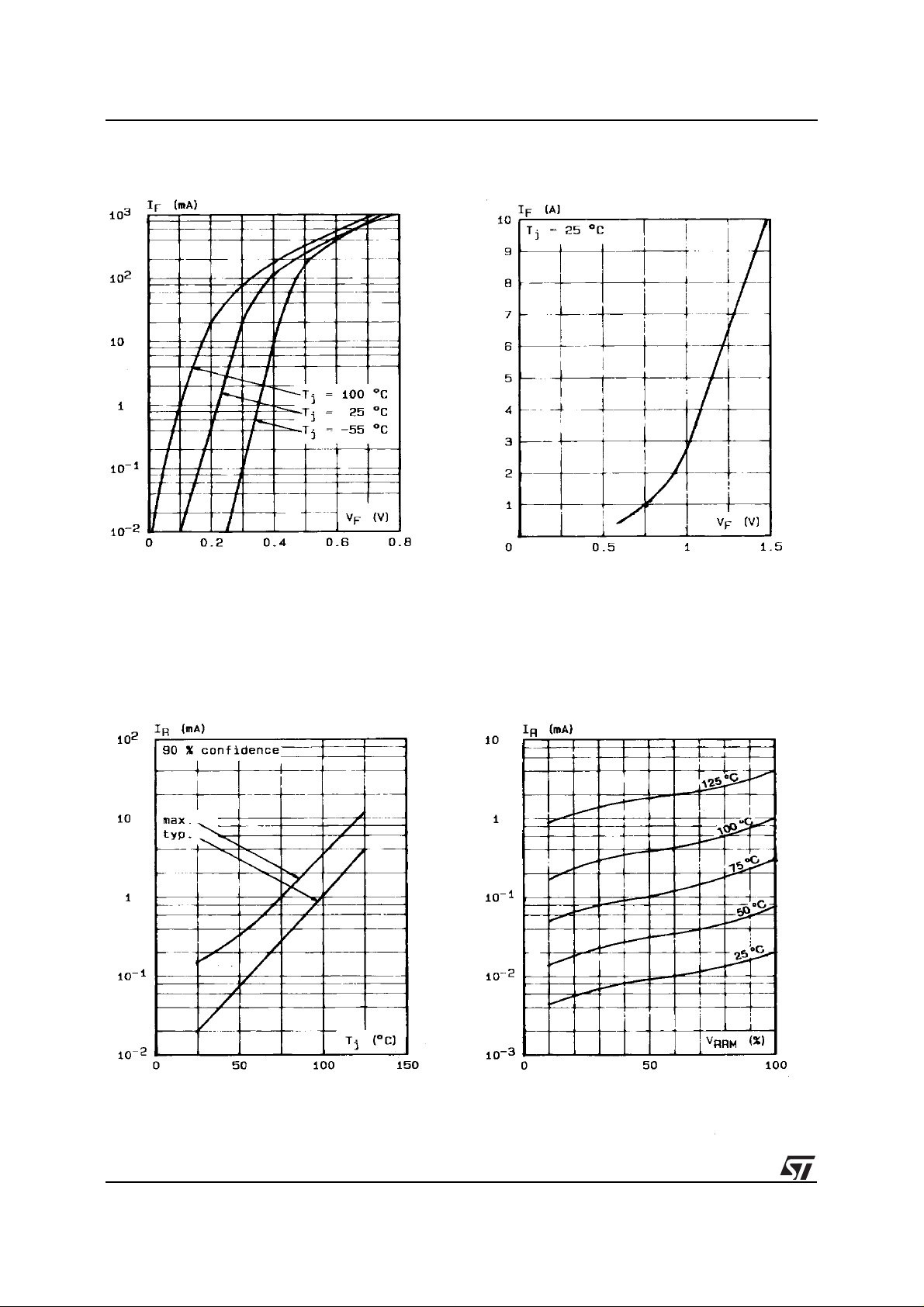
Figure 1. Forward current versus forward
voltage at low level (typical values).
Figure 2. Forward current versus forward
voltage at high level (typical values).
Figure 3. Reverse current versus junction
temperature.
Figure 4. Reverse current versus V
cent.
RRM
in per
2/4

BAT 49
Figure 5. Capacitance C versus reverse
applied voltage V
(typical values).
R
Figure 6. Surge non repetitive forward current
for a rectangular pulse with t ≤ 10 ms.
Figure 7. Surge non repetitive forward current
versus number of cycles.
3/4

BAT 49
PACKAGE MECHANICAL DATA
DO 41 Glass
BA B
note 1
E
/
O
D
note 2
Cooling method : by convection and conduction
Marking: clear, ring at cathode end.
Weight: 0.34g
E
O
/
note 1
D
/
O
C
DIMENSIONS
REF.
Millimeters Inches
Min. Max. Min. Max.
A 4.07 5.20 0.160 0.205
B 2.04 2.71 0.080 0.107
C28 1.102
D 0.712 0.863 0.028 0.034
Information furnished is believed to be accurate and reliable. However, STMicroelectronics assumes no responsibility for t he c on sequences of
use of such information nor for any infri ngem ent of patents or other rights of third parties which may result from its use. No license is granted
by implication or otherwise under any patent or patent rights of STMicroelectronics. Specifications mentioned in this publication are subject to
change without notice. This publication supersedes and replaces all information previously supplied.
STMicroelectronics products are not authorized for use as critical components in life support devices or systems without express written approval
of STMicroelectronic s.
The ST logo is a registered trademark of STMicroelectronics
© 1999 STMicroelectronics - Printed in Italy - All rights reserved.
STMicroelectronics GROUP OF COMPANIES
Australia - Brazil - China - Finland - France - Germany - Hong Kong - India - Italy - Japan - Malaysia
Malta - Morocco - Singapore - Spain - Sweden - Switzerland - United Kingdom - U.S.A.
http://www.st.com
4/4
 Loading...