

Page 1
Features
■ very low conduction losses
■ negligible switching losses
■ low capacitance diode
■ Flip Chip, 2-bump package
BAT30F3
Small signal Schottky diode
Complies with the following standards
■ IEC 61000-4-2 level 1:
– ±2kV (air discharge)
– ±2kV (contact discharge)
Description
The BAT30F3 is a Schottky diode in a 2-bump,
Flip-Chip package.
This device is specially suited for switching mode
applications needing a low forward voltage drop
diode.
The electrical parameters are guaranteed across
the operating temperature range
(- 30 °C to 85 °C).
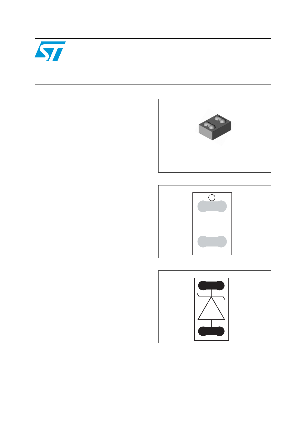
Flip Chip
(2 bumps)
Figure 1. Pin configuration (bump side)
1
A
B
Figure 2. Schematic
1
A
B
October 2010 Doc ID 16915 Rev 2 1/10
www.st.com
10
Page 2
Characteristics BAT30F3
1 Characteristics
Table 1. Absolute maximum ratings (T
Symbol Parameter Value Unit
Peak pulse voltage:
V
PP
IEC 61000-4-2 air discharge
IEC 61000-4-2 contact discharge
amb
= 25 °C)
±2
±2
kV
V
T
1. condition to avoid thermal runaway for a diode on its own heatsink
Table 2. Electrical characteristics
Repetitive peak reverse voltage 20 V
RRM
Storage temperature range
stg
Operating junction temperature range -30 to +85 °C
T
op
<
Rth(j-a)
1
dPtot
dTj
(1)
-55 to +150 °C
Symbol Parameter Test conditions Min. Typ. Max. Unit
VR = 6 V - - 2
25 °C
= 20 V - - 6
V
R
V
= 6 V - - 20
(1)
I
Reverse leakage current
R
V
Forward voltage drop
F
1. Pulse test: tp = 5 ms, δ < 2%
55 °C
85 °C
25 °C
- 30 °C
R
V
= 20 V - - 55
R
V
= 6 V - - 145
R
= 20 V - - 360
V
R
I
= 0.1 mA - - 200
F
= 1 mA - - 270
I
F
= 10 mA - - 340
I
F
I
= 100 mA - - 440
F
= 200 mA - - 500
I
F
= 300 mA - - 560
I
F
I
= 0.1 mA - - 300
F
= 1 mA - - 355
I
F
= 10 mA - - 415
I
F
I
= 100 mA - - 495
F
= 200 mA - - 545
I
F
= 300 mA - - 600
I
F
mV
µA
2/10 Doc ID 16915 Rev 2
Page 3
BAT30F3 Characteristics
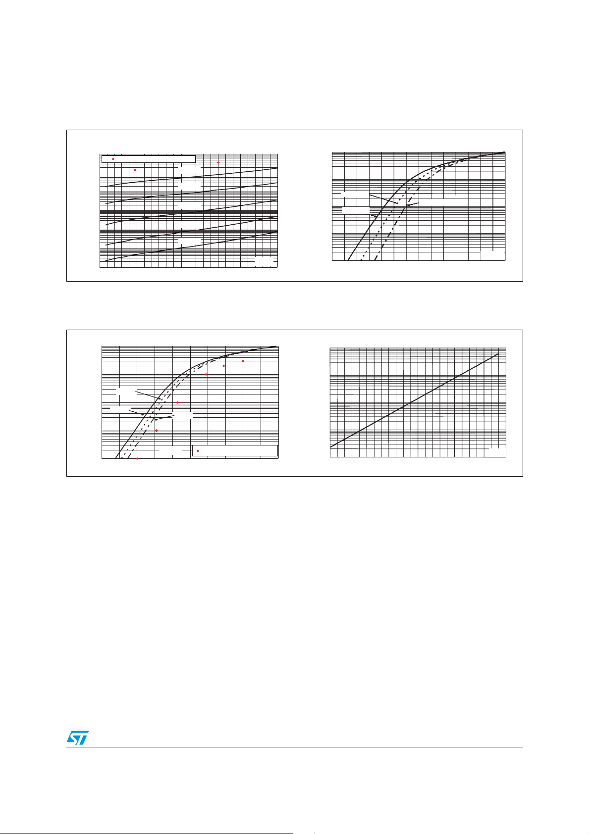
Figure 3. Leakage current versus reverse
applied voltage (typical values)
I (µA)
R
1.E+03
1.E+02
1.E+01
1.E+00
1.E-01
1.E-02
1.E-03
Tj=85°C (Maximum specified values)
Tj=85°C
Tj=55°C
Tj=25°C
Tj=0°C
Tj=-30°C
V (V)
R
0 5 10 15 20 25 30
Figure 5. Forward voltage drop versus
forward current (typical values,
negative temperatures)
I (A)
FM
1.E+00
1.E-01
Tj=-20°CTj=-20°C
1.E-02
1.E-03
Tj=-10°CTj=-10°C
Tj=-30°CTj=-30°C
Figure 4. Forward voltage drop versus
forward current (typical values,
positive temperatures)
I (A)
FM
1.E+00
1.E-01
1.E-02
Tj= 55 °C
Tj= 85 °C
Tj= 25 °C
1.E-03
1.E-04
0.0 0.1 0.2 0.3 0.4 0.60.5 0.7
V (V)
Figure 6. Relative variation of reverse
leakage current versus junction
temperature (typical values)
I[Tj] / I [Tj= 25 °C]
RR
1.E+02
1.E+01
1.E+00
1.E-01
FM
V (V)
1.E-04
0.2 0.3 0.4 0.5 0.6 0.7
FM
Tj=-30°C (Maximum specified values)
1.E-02
-30 -20 0 20 40 60 80-10 10
30
Tj(°C)
50 70 90
Doc ID 16915 Rev 2 3/10
Page 4

Ordering information scheme BAT30F3
2 Ordering information scheme
Figure 7. Ordering information scheme
BAT30 F3
Signal Schottky diode
V = 20 V
RRM
Package
F = Flip Chip
x = 3: lead-free, pitch = 400 µm
4/10 Doc ID 16915 Rev 2
Page 5

BAT30F3 Package information
3 Package information
● Epoxy meets UL94, V0
● Lead-free packages
In order to meet environmental requirements, ST offers these devices in different grades of
ECOPACK
specifications, grade definitions and product status are available at: www.st.com
ECOPACK
®
packages, depending on their level of environmental compliance. ECOPACK®
®
is an ST trademark.
.
Figure 8. Package dimensions (dimensions in mm)
0.50
0.37
0.065
0.70
0.40
G
R 0.09
G
0.06
0.12
0.28
0.085
Section G-G
Doc ID 16915 Rev 2 5/10
Page 6

PCB recommendations BAT30F3
Figure 9. Flip Chip tape and reel specification (dimensions in mm)
0.20 ± 0.05
0.75 ± 0.05
8.0 ± 0.3
0.43 ± 0.1
All dimensions in mm
3
4 PCB recommendations
4.1 Design
3
4.0 ± 0.1
3
2.0 ± 0.05
3
0.57 ± 0.05
User direction of unreeling
3
2.0 ± 0.1
Ø 1.55 ± 0.05
3
3
1.75 ± 0.1
3.5 ±- 0.05
For optimum electrical performance and highly reliable solder joints, STMicroelectronics
recommends the PCB design recommendations listed in Tabl e 3 .
Table 3. PCB design recommendations for solder bar pitch 400 µm
Oblong pad: 370 x 180 µm
– Micro via SSBU allowed
– Micro via SBU to be avoided
For NSMD PCB
non solder mask defined
– Micro via SBU filled (under qualification)
Tr a ck :
– Only one track per pad
– Maximum track width = 100 µm
Track layout must be symmetrical to the die axis (to homogenize stress
and welding attraction during reflow assembly)
Oblong pad:
For SMD PCB
solder mask defined
– Micro via SSBU allowed
– Micro via SBU to be avoided
– Micro via SBU filled (under qualification)
PCB Pad Finishing Cu – Ni (2-6 µm) - Au (0.2 µm max)
Note: A gold layer finishing on the PCB pad that is too thick (0.2 µm maximum) is not
recommended (low joint reliability).
6/10 Doc ID 16915 Rev 2
Page 7

BAT30F3 PCB recommendations
To optimize the natural self centering effect of CSP on the PCB, PCB pad positioning and
size have to be properly designed (see Figure 10)
Micro vias
An alternative to routing on the top surface is to route out on buried layers. To achieve this,
the pads are connected to the lower layers using micro vias. Only SSBU via technology is
approved.
Figure 10. Solder mask opening
450 µm
370 µm
370 µm
255 µm
180 µm
Non solder mask defined
180 µm
100 µm
Solder mask defined
Doc ID 16915 Rev 2 7/10
Page 8

PCB recommendations BAT30F3
4.2 Assembly
For chip scale package mounting on the PCB, STMicroelectronics recommends the use of a
solder stencil aperture of 330 x 330 µm maximum and a typical stencil thickness of 75 or
80 µm. Chip scale packages are fully compatible with the use of near eutectic 95.5 Sn, 4 Ag,
0.5 Cu solder paste with no-clean flux. ST's recommendations for chip scale package board
mounting are illustrated on the soldering reflow profile shown in Figure 11.
Figure 11. ST ECOPACK
Temperature (°C)
Temperature (°C)
260°C max
260°C max
255°C
255°C
220°C
220°C
180°C
180°C
125 °C
125 °C
3°C/s max
3°C/s max
0
0
012345 67
012345 67
®
recommended soldering reflow profile for PCB mounting
2°C/s recommended
90 to 150 sec
90 to 150 sec
10-30 sec
10-30 sec
90 sec max
90 sec max
2°C/s recommended
6°C/s max
6°C/s max
Time (min)
Time (min)
Dwell time in the soldering zone (with temperature higher than 220 °C) has to be kept as
short as possible to prevent component and substrate damage. Peak temperature must not
exceed 260 °C. Controlled atmosphere (N2 or N2H2) is recommended during the whole
reflow, especially above 150 °C.
Chip scale packages are able to withstand three times the previous recommended reflow
profile in order to be compatible with a double reflow when SMDs are mounted on both sides
of the PCB and one additional repair.
A maximum of three soldering reflows are allowed for these lead-free packages (with repair
step included).
The use of a no-clean flux is highly recommended to avoid any cleaning operation. To
prevent any bump cracks, ultrasonic cleaning methods are not recommended.
8/10 Doc ID 16915 Rev 2
Page 9

BAT30F3 Ordering information
5 Ordering information
Table 4. Ordering information
Order code Marking Package Weight Base qty Delivery mode
BAT30F3 3 Flip Chip 0.3 mg 15000 Tape and reel 7”
6 Revision history
Table 5. Document revision history
Date Revision Changes
14-Dec-2009 1 Initial release.
21-Oct-2010 2 Updated dot graphic in Figure 1.
Doc ID 16915 Rev 2 9/10
Page 10

BAT30F3
Please Read Carefully:
Information in this document is provided solely in connection with ST products. STMicroelectronics NV and its subsidiaries (“ST”) reserve the
right to make changes, corrections, modifications or improvements, to this document, and the products and services described herein at any
time, without notice.
All ST products are sold pursuant to ST’s terms and conditions of sale.
Purchasers are solely responsible for the choice, selection and use of the ST products and services described herein, and ST assumes no
liability whatsoever relating to the choice, selection or use of the ST products and services described herein.
No license, express or implied, by estoppel or otherwise, to any intellectual property rights is granted under this document. If any part of this
document refers to any third party products or services it shall not be deemed a license grant by ST for the use of such third party products
or services, or any intellectual property contained therein or considered as a warranty covering the use in any manner whatsoever of such
third party products or services or any intellectual property contained therein.
UNLESS OTHERWISE SET FORTH IN ST’S TERMS AND CONDITIONS OF SALE ST DISCLAIMS ANY EXPRESS OR IMPLIED
WARRANTY WITH RESPECT TO THE USE AND/OR SALE OF ST PRODUCTS INCLUDING WITHOUT LIMITATION IMPLIED
WARRANTIES OF MERCHANTABILITY, FITNESS FOR A PARTICULAR PURPOSE (AND THEIR EQUIVALENTS UNDER THE LAWS
OF ANY JURISDICTION), OR INFRINGEMENT OF ANY PATENT, COPYRIGHT OR OTHER INTELLECTUAL PROPERTY RIGHT.
UNLESS EXPRESSLY APPROVED IN WRITING BY AN AUTHORIZED ST REPRESENTATIVE, ST PRODUCTS ARE NOT
RECOMMENDED, AUTHORIZED OR WARRANTED FOR USE IN MILITARY, AIR CRAFT, SPACE, LIFE SAVING, OR LIFE SUSTAINING
APPLICATIONS, NOR IN PRODUCTS OR SYSTEMS WHERE FAILURE OR MALFUNCTION MAY RESULT IN PERSONAL INJURY,
DEATH, OR SEVERE PROPERTY OR ENVIRONMENTAL DAMAGE. ST PRODUCTS WHICH ARE NOT SPECIFIED AS "AUTOMOTIVE
GRADE" MAY ONLY BE USED IN AUTOMOTIVE APPLICATIONS AT USER’S OWN RISK.
Resale of ST products with provisions different from the statements and/or technical features set forth in this document shall immediately void
any warranty granted by ST for the ST product or service described herein and shall not create or extend in any manner whatsoever, any
liability of ST.
ST and the ST logo are trademarks or registered trademarks of ST in various countries.
Information in this document supersedes and replaces all information previously supplied.
The ST logo is a registered trademark of STMicroelectronics. All other names are the property of their respective owners.
© 2010 STMicroelectronics - All rights reserved
Australia - Belgium - Brazil - Canada - China - Czech Republic - Finland - France - Germany - Hong Kong - India - Israel - Italy - Japan -
STMicroelectronics group of companies
Malaysia - Malta - Morocco - Philippines - Singapore - Spain - Sweden - Switzerland - United Kingdom - United States of America
www.st.com
10/10 Doc ID 16915 Rev 2
 Loading...