

®
BAT20J
HIGH EFFICIENCY SWITCHING AND
ULTRA LOW LEAKAGE CURRENT SCHOTTKY DIODE
MAIN PRODUCT CHARACTERISTICS
I
F(AV)
V
RRM
25°C(max) @ 15V 12 µA
I
R
1A
23 V
Tj (max) 150 °C
FEATURES AND BENEFITS
Low conduction losses
■
Very low reverse current
■
Negligible switching losses
■
Low capacitance diode
■
Low forward and reverse recovery times
■
Extremely fast switching
■
Surface mount device
■
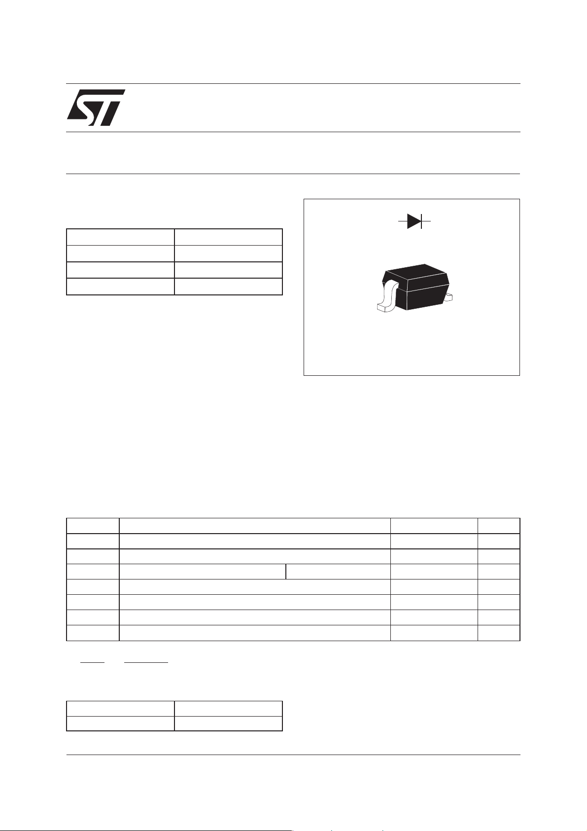
DESCRIPTION
The BAT20J is using 23V schottky barrier diode
encapsulated on a SOD-323 package. This is specially suited for switching mode in mobile phone
and PDA power management applications or LED
driver circuits (step up converters).
AK
SOD-323
ABSOLUTE RATINGS (limiting values)
Symbol Parameter Value Unit
V
RRM
I
F(RMS)
I
F(AV)
I
FSM
T
stg
Repetitive peak reverse voltage 23 V
Repetitive peak forward current 2 A
Average forward current δ = 0.38 1 A
Surge non repetitive forward current (tp=10ms sinusoidal) 5 A
Maximum storage temperature range - 65 to +150 °C
Tj Maximum operating junction temperature * 150 °C
TL Maximum temperature for soldering during * 260 °C
dPtot
*:
<
dTj Rth j a
thermal runaway condition for a diode on its own heatsink
−1()
Order code
Part Number Marking
BAT20JFILM 20
April 2004 - Ed: 1
1/5
BAT20J
THERMAL RESISTANCE
Symbol Parameter Value Unit
R
th (j-a)
(*) Mounted on epoxy board without copper heat sink.
Junction to Ambient (*) 600 °C/W
STATIC ELECTRICAL CHARACTERISTICS
Symbol Parameters Tests conditions Min. Typ. Max. Unit
I
* Reverse leakage current
R
Tj = 25°C VR=5V
(see note 1)
* Reverse leakage current Tj = 85°C VR=5V
I
R
** Forward voltage drop Tj = 25°C IF=10mA
V
F
* Pulse test tp = 380 µs, δ <2%
** Pulse test tp = 5 ms, δ <2%
Note 1: I
at 23 V and Tj = 25°C is equal to 60 µA typ.
R
V
=8V
R
V
=15V
R
V
=8V
R
V
=15V
R
I
= 100 mA
F
I
=1A
F
0.65
0.88
3.00
55
70
120
0.28
0.35
0.54
2
3
12
120
150
250
0.31
0.40
0.62
µA
DYNAMIC ELECTRICAL CHARACTERISTICS
Symbol Parameters Tests conditions Min. Typ. Max. Unit
V
C
To evaluate the maximum conduction losses, use the following equations :
P = 0.32 x I
Diode capacitance VR=5V F=1MHz 20 30 pF
d
+ 0.23 x I
F(AV)
F2(RMS)
2/4

BAT20J
Fig. 1: Peak forward current versus ambient
temperature (δ = 0.11).
I(A)
P
3.0
2.5
2.0
1.5
1.0
δ
=tp/T
T
T (°C)
tp
amb
0.5
0.0
0 25 50 75 100 125 150
Printed circuit board FR4
S =2.25mm
CU
2
Fig. 3: Relative variation of thermal impedance
junction to ambient versus pulse duration .
Z/R
th(j-a) th(j-a)
1.E+00
1.E-01
Single pulse
S =2.25mm
CU
2
Fig. 2: Average forward current versus ambient
temperature ( δ = 0.5).
I(A)
F(AV)
0.40
0.35
0.30
0.25
0.20
0.15
0.10
0.05
0.00
0 25 50 75 100 125 150
δ
=tp/T
T
T (°C)
tp
amb
Printed circuit board FR4
S =2.25mm
CU
2
Fig. 4: Reverse leakage currrent versus reverse
voltage applied (typical values).
I (µA)
R
1.E+04
1.E+03
1.E+02
T =150°C
j
T =85°C
j
1.E-02
t(s)
1.E-03
1.E-03 1.E-02 1.E-01 1.E+00 1.E+01 1.E+02 1.E+03
p
Fig. 5: Relative variation of reverse leakage
currrent versus junction temperature (typical
values).
I(T
) / =25°CI(T )
Rj Rj
1.E+04
1.E+03
1.E+02
1.E+01
1.E+00
1.E-01
V =5V
R
T (°C)
j
0 25 50 75 100 125 150
1.E+01
T =25°C
j
1.E+00
V (V)
1.E-01
0 2 4 6 8 1012141618 202224
R
Fig. 6: Junction capacitance versus reverse
voltage applied (typical values).
C(pF)
100
10
V (V)
1
1 10 100
R
F=1MHz
V =30mV
OSC RMS
T =25°C
j
3/5

BAT20J
Fig. 7-1: Forward voltage drop versus forward
current (typical values, high level).
I(A)
FM
1.E+01
T =150°C
1.E+00
1.E-01
1.E-02
1.E-03
1.E-04
0.0 0.1 0.2 0.3 0.4 0.5 0.6 0.7 0.8 0.9 1.0 1.1 1.2 1.3
j
T =85°C
j
T =25°C
j
V(V)
FM
Fig. 8: Thermal resistance junction to ambient
versus copper surface under tab (epoxy
printed circuit board FR4, e
=35µm, typical
CU
values).
R(°C/W)
th(j-a)
600
550
500
450
400
350
300
250
200
150
100
50
0
0 5 10 15 20 25 30 35 40 45 50
S(mm
²)
Cu
Fig. 7-2: Forward voltage drop versus forward
current (low level).
I(A)
FM
1.0
0.9
0.8
0.7
0.6
0.5
0.4
0.3
0.2
0.1
0.0
0.0 0.1 0.2 0.3 0.4 0.5 0.6 0.7
T =85°C
j
(typical values)
T =150°C
j
(typical values)
(maximum values)
V(V)
FM
T =25°C
j
(typical values)
T =25°C
j
Fig. 9: Thermal resistance junction to ambient
versus power dissipation (epoxy printed circuit
board FR4, e
R (°C/W)
th(j-a)
700
650
600
550
500
450
400
350
300
250
200
150
100
50
0
0 50 100 150 200 250 300 350 400
=35µm, typical values).
CU
P(mW)
S =2.25mm
CU
T =25°C
amb
2
4/5

PACKAGE MECHANICAL DATA
SOD-323
H
b
A1
REF.
BAT20J
DIMENSIONS
Millimeters Inches
Min. Max. Min. Max.
E
A 1.13 0.045
A1 0 0.1 0 0.004
b 0.25 0.44 0.01 0.017
D
c
Q1
A
c 0.1 0.25 0.004 0.01
D 1.52 1.8 0.06 0.071
E 1.11 1.35 0.044 0.053
H 2.3 2.7 0.09 0.106
L
L 0.1 0.46 0.004 0.02
Q1 0.1 0.41 0.004 0.016
Ordering type Marking Package Weight Base qty Delivery mode
BAT20JFILM 20 SOD-323 0.005g 3000 Tape & reel
■
Epoxy meets UL94,V0
Information furnished is believed to be accurate and reliable. However, STMicroelectronics assumes no responsibility for the consequences of
use of such information nor for any infringement of patents or other rights of third parties which may result from its use. No license is granted by
implication or otherwise under any patent or patent rights of STMicroelectronics. Specifications mentioned in this publication are subject to
change without notice. This publication supersedes and replaces all information previously supplied. STMicroelectronics products are not au
thorized for use as critical components in life support devices or systems without express written approval of STMicroelectronics.
The ST logo is a registered trademark of STMicroelectronics.
All other names are the property of their respective owners.
© 2004 STMicroelectronics - All rights reserved.
STMicroelectronics GROUP OF COMPANIES
Australia - Belgium - Brazil - Canada - China - Czech Republic - Finland - France - Germany -
Hong Kong - India - Israel - Italy - Japan - Malaysia - Malta - Morocco - Singapore - Spain -
Sweden - Switzerland - United Kingdom - United States
www.st.com
5/5
-
 Loading...