

Page 1
BAS70
Low capacitance, low series inductance and resistance Schottky diodes
Features
■ Very low conduction losses
■ Negligible switching losses
■ Low forward and reverse recovery times
■ Surface mount device
■ Low capacitance diode
■ Low resistance and inductance
Description
The BAS70 series uses 70 V Schottky barrier
diodes packaged in SOD-123, SOD-323, SOD523, SOT-23, SOT-323, SOT-323-6L or SOT-666.
These diodes are specially suited for signal
detection and temperature compensation in RF
applications.
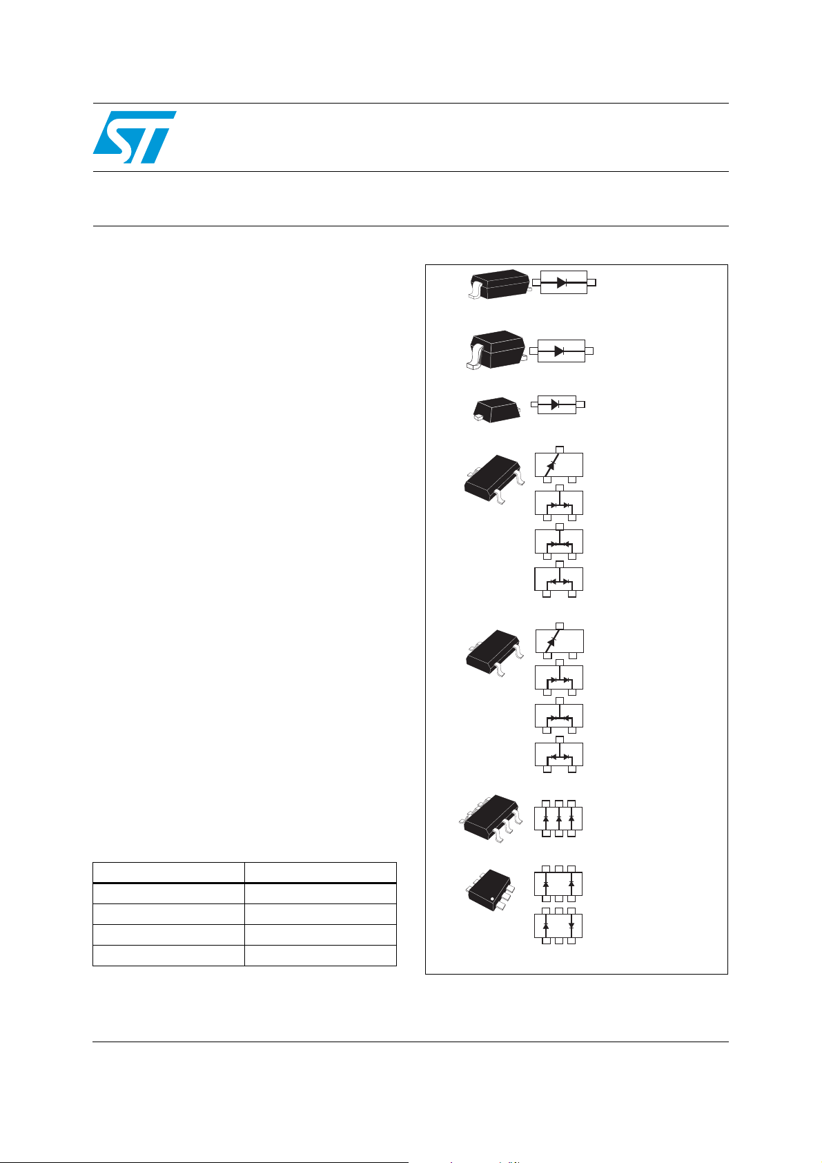
SOD-123
SOD-323
SOD-523
SOT-23
SOT-323
BAS70ZFILM
(Single)
BAS70JFILM
(Single)
BAS70KFILM
(Single)
BAS70FILM
(Single)
BAS70-04FILM
(Series)
BAS70-05FILM
(Common cathode)
BAS70-06FILM
(Common anode)
BAS70WFILM
(Single)
BAS70-04WFILM
(Series)
BAS70-05WFILM
(Common cathode)
BAS70-06WFILM
(Common anode)
BAS70-08SFILM
(3 parallel diodes)
Table 1. Device summary
Symbol Value
I
F
V
RRM
(max) 2 pF
C
(max) 150 °C
T
j
70 mA
70 V
SOT-323-6L
SOT-666
BAS70-07P6FILM
(2 parallel diodes)
BAS70-09P6FILM
(2 opposite diodes)
Configurations in top view
October 2009 Doc ID 12563 Rev 2 1/14
www.st.com
14
Page 2
Characteristics BAS70
1 Characteristics
Table 2. Absolute ratings (limiting values at Tj = 25 °C, unless otherwise specified)
Symbol Parameter Value Unit
V
I
T
Table 3. Thermal parameters
Repetitive peak reverse voltage 70 V
RRM
I
Continuous forward current 70 mA
F
Surge non repetitive forward current tp = 10 ms Sinusoidal 1 A
FSM
Storage temperature range - 65 to +150 °C
stg
T
Maximum operating junction temperature 150 °C
j
Maximum soldering temperature 260 °C
T
L
Symbol Parameter Value Unit
SOD-123, SOT-23 500
R
Junction to ambient
th(j-a)
(1)
°C/WSOT-323, SOD-323 550
SOD-523, SOT-666 600
1. Epoxy printed circuit board with recommended pad layout
Table 4. Static electrical characteristics
Symbol Parameter Test conditions Min. Typ. Max. Unit
V
= 50 V 100 nA
(1)
I
V
1. Pulse test: tp = 5 ms, δ < 2 %
2. Pulse test: tp = 380 µs, δ < 2 %
Table 5. Dynamic characteristics
Symbol Parameter
Reverse leakage current Tj = 25 °C
R
(2)
Forward voltage drop Tj = 25 °C
F
Test conditions
R
V
= 70 V 10
R
I
= 1 mA 410
F
= 10 mA 750
F
I
= 15 mA 1000
F
Min. Typ. Max. Unit
µA
mVI
C Diode capacitance V
Differential forward
R
F
resistance
L
Series inductance 1.5 nH
S
= 0 V, F = 1 MHz 2 pF
R
I
= 10 mA, F = 100 MHz 30 Ω
F
2/14 Doc ID 12563 Rev 2
Page 3
BAS70 Characteristics
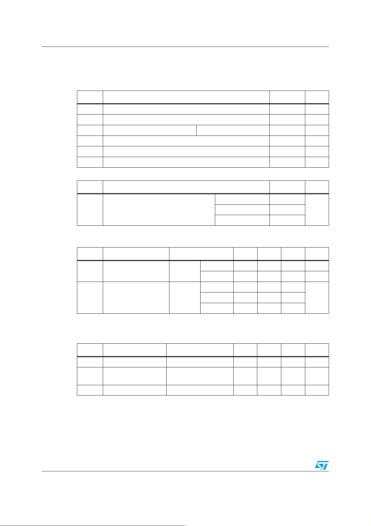
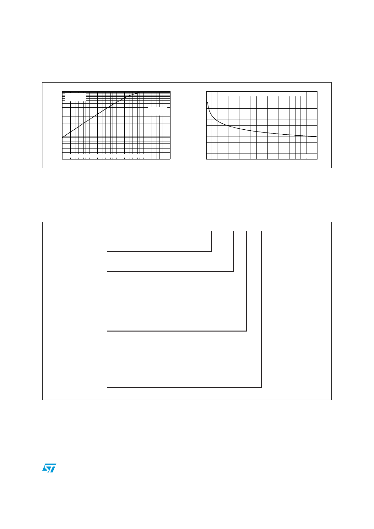
Figure 1. Average forward power dissipation
versus average forward current
P(W)
0.14
0.12
0.10
0.08
0.06
0.04
0.02
0.00
0.00 0.01 0.02 0.03 0.04 0.05 0.06 0.07 0.08 0.09 0.10
d=0.05
d=0.1
d=0.2
d=0.5
d=1
T
tp
=tp/T
I
(A)
F(AV)
d
Figure 3. Reverse leakage current versus
reverse applied voltage
(typical values)
IR(µA)
1.E+02
1.E+01
1.E+00
1.E-01
1.E-02
1.E-03
0 10203040506070
Tj=150 °C
Tj=85 °C
Tj=25 °C
VR(V)
Figure 2. Average forward current versus
ambient temperature (δ = 1)
I
(A)
F(AV)
0.08
0.07
0.06
0.05
0.04
0.03
0.02
0.01
0.00
0 25 50 75 100 125 150
d
=tp/T
T
tp
T
(°C)
amb
Figure 4. Reverse leakage current versus
junction temperature
(typical values)
IR(µA)
1.E+02
VR=50 V
1.E+01
1.E+00
1.E-01
1.E-02
0 25 50 75 100 125 150
Tj(°C)
Figure 5. Junction capacitance versus
reverse applied voltage
(typical values)
C(pF)
10.0
1.0
0.1
0.1 1.0 10.0 100.0
VR(V)
V
OSC
F=1 MHz
=30 mV
Tj=25 °C
Figure 6. Forward voltage drop versus
forward current (typical values)
IFM(mA)
1.E+02
RMS
Doc ID 12563 Rev 2 3/14
Tj=150 °C
1.E+01
Tj=-40 °CTj=-40 °C
1.E+00
Tj=85°CTj=85°C
1.E-01
0.0 0.5 1.0 1.5 2.0 2.5 3.0 3.5
VFM(V)
Page 4
Characteristics BAS70
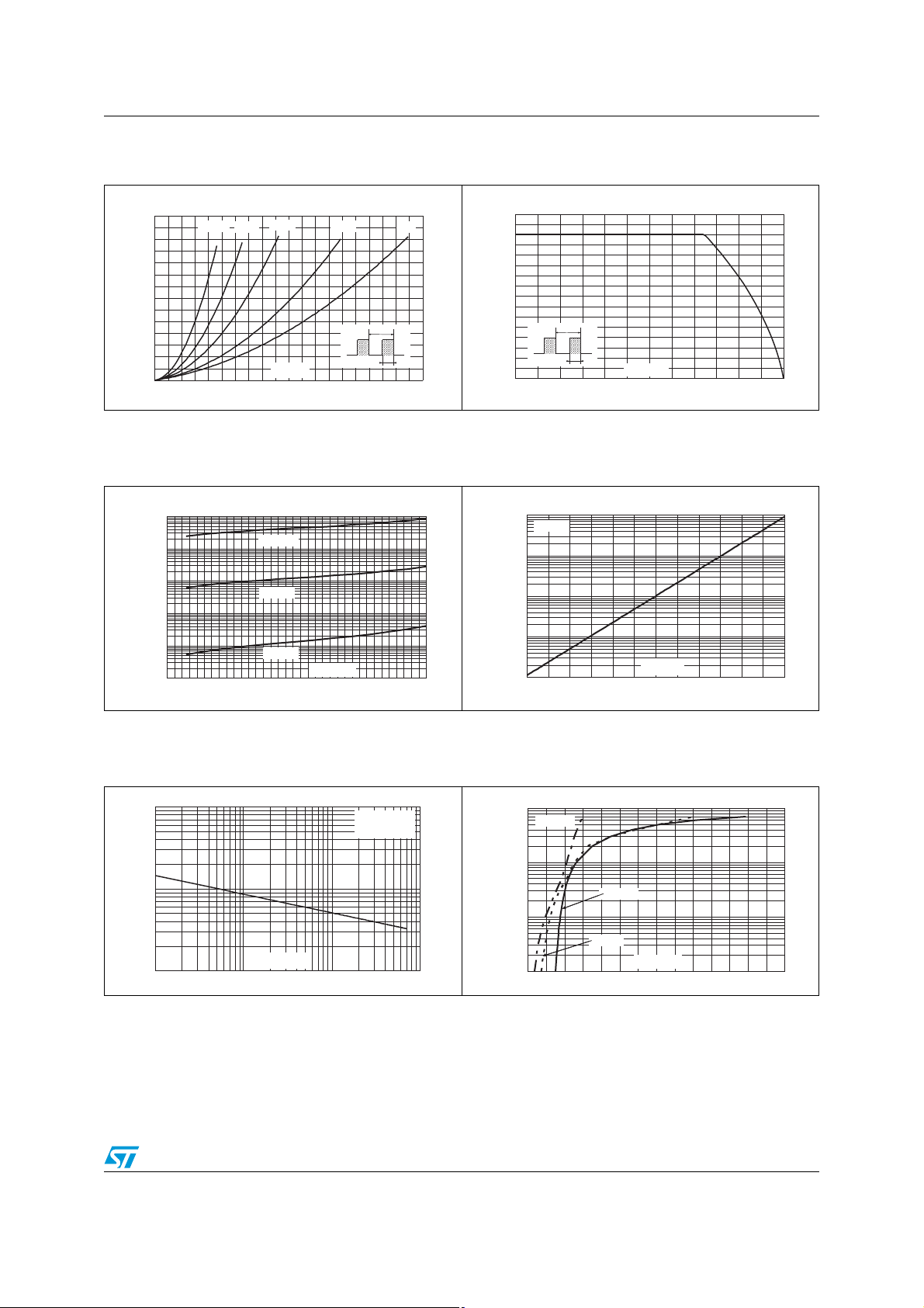
2
Figure 7. Forward voltage drop versus
forward current (typical values)
IFM(mA)
1.E+02
1.E+01
1.E+00
1.E-01
Tj=125 °C
Tj=25 °C
VFM(V)
0.0 0.5 1.0 1.5 2.0 2.5 3.0 3.5
Figure 9. Relative variation of thermal
impedance junction to ambient
versus pulse duration
Z
(°C/W)
th(j-a)
1000
printed circuit board, epoxy FR4 e = 35 µm SOT-323-6L
100
CU
Single pulse
SOT-323-6L
Figure 8. Differential forward resistance
versus forward current
(typical values)
R()FΩ
1000
100
10
0.1 1.0 10.0
IF(mA)
F=100 MHz
Tj=25 °C
Figure 10. Relative variation of thermal
impedance junction to ambient
versus pulse duration
Z
th(j-a)/Rth(j-a)
1.00
Single pulse
SOT-23
Aluminesubstrate
0.10
10 x 8 x 0.5 mm
10
1.E-02 1.E-01 1.E+00 1.E+01 1.E+02
tP(s)
Figure 11. Relative variation of thermal
impedance junction to ambient
versus pulse duration
Z
th(j-a)/Rth(j-a)
1.00
Single pulse
SOD-323
EpoxyFR4
S
=2.25 mm²
CU
e
=35 µm
0.10
printed circuit board, epoxy FR4 e = 35 µm SOD-323
0.01
1.E-02 1.E-01 1.E+00 1.E+01 1.E+02
CU
CU
tP(s)
alluminium oxide substrate 10 x 8 x 0.5 mm SOT-23
0.01
1.E-02 1.E-01 1.E+00 1.E+01 1.E+0
Figure 12. Relative variation of thermal
impedance junction to ambient
versus pulse duration
Z
th(j-a)/Rth(j-a)
1.00
Single pulse
SOT-666
Epoxy FR4
=35 µm
e
0.10
printed circuit board, epoxy FR4 e = 35 µm SOT-666
0.01
1.E-03 1.E-02 1.E-01 1.E+00 1.E+01
CU
CU
tP(s)
tP(s)
4/14 Doc ID 12563 Rev 2
Page 5
BAS70 Ordering information scheme
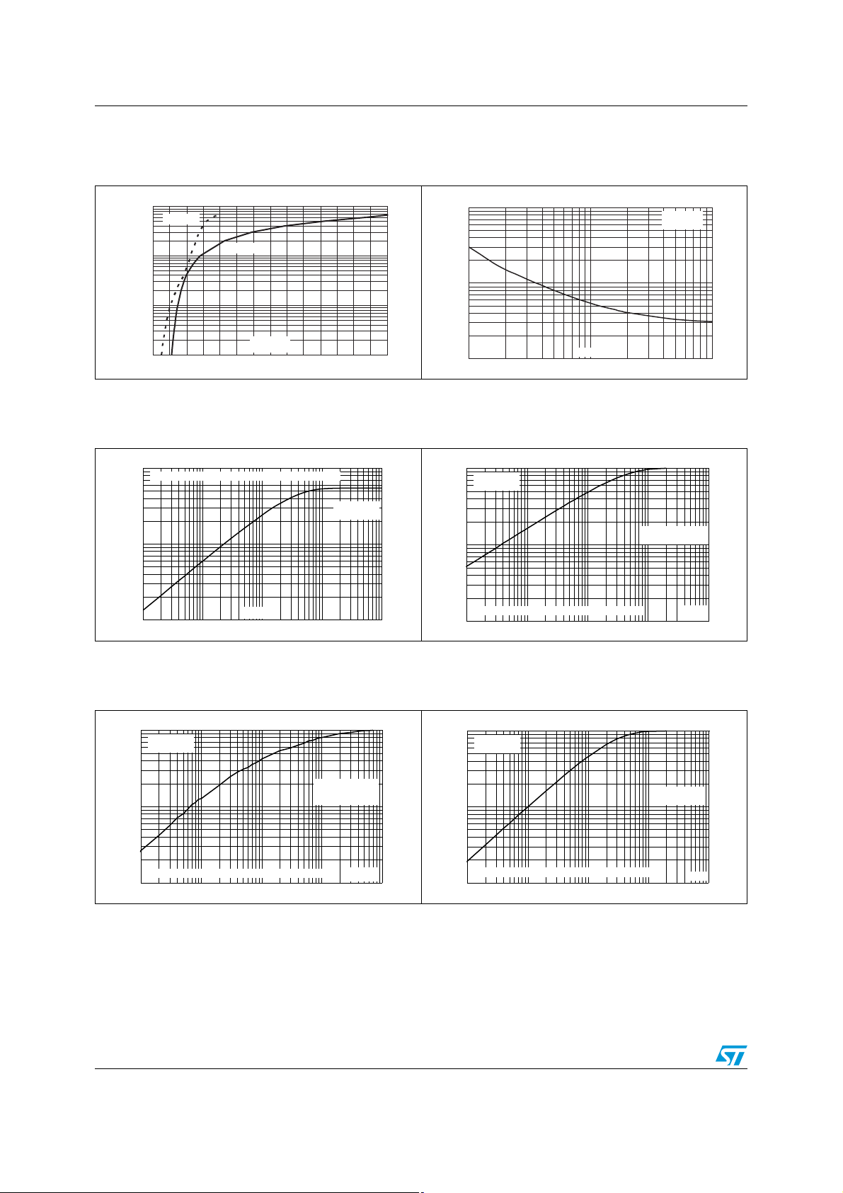
Figure 13. Relative variation of thermal
Figure 14. Thermal impedance junction to
impedance junction to ambient
versus pulse duration
Z
th(j-a)/Rth(j-a)
1.00
Single pulse
SOD-523
EpoxyFR4
e
=35 µm
0.10
0.01
printed circuit board, epoxy FR4 e = 35 µm SOD-523
0.00
1.E-03 1.E-02 1.E-01 1.E+00 1.E+01
CU
CU
tP(s)
R
th(j-a)
600
550
500
450
400
350
300
0 5 10 15 20 25 30 35 40 45 50
2 Ordering information scheme
Figure 15. Ordering information scheme
BAS70 xx xx FILM
ambient versus copper surface
under each lead
(°C/W)
printed circuit board, epoxy FR4 e = 35 µm SOD-323
CU
SCU(mm²)
Signal Schottky diodes
V=70V
RRM
Configuration
No letter = Single diode
04 = Series diodes
05 = Common cathode
06 = Common anode
07 = 2 Parallel diodes
08 = 3 Parallel diodes
09 = 2 Opposite diodes
Package
Blank = SOT-23
J = SOD-323
W = SOT-323
K = SOD-523
P6 = SOT-666
S = SOT323-6L
Z = SOD-123
Packing
FILM = Tape and reel
Doc ID 12563 Rev 2 5/14
Page 6

Package information BAS70
3 Package information
● Epoxy meets UL94, V0
● Lead-free packages
In order to meet environmental requirements, ST offers these devices in different grades of
ECOPACK
specifications, grade definitions and product status are available at: www.st.com
ECOPACK
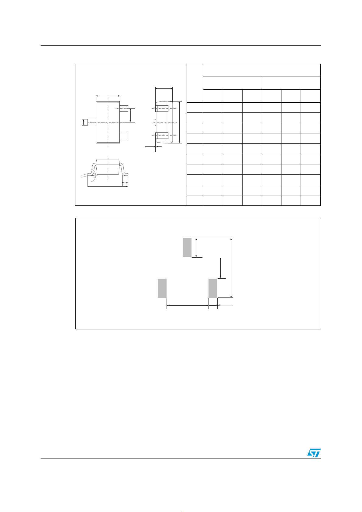
Table 6. SOD-123 dimensions
®
packages, depending on their level of environmental compliance. ECOPACK®
®
is an ST trademark.
.
Dimensions
H
b
E
A2
Ref.
A1
A 1.45 0.057
Millimeters Inches
Min. Max. Min. Max.
A1 0 0.1 0 0.004
D
A
A2 0.85 1.35 0.033 0.053
b 0.55 Typ. 0.022 Typ.
c
c 0.15 Typ. 0.039 Typ.
D 2.55 2.85 0.1 0.112
E 1.4 1.7 0.055 0.067
G
G0.25 0.01
H 3.55 3.95 0.14 0.156
Figure 16. SOD-123 footprint (dimensions in mm)
4.45
2.510.97 0.97
6/14 Doc ID 12563 Rev 2
0.65
Page 7

BAS70 Package information
Table 7. SOD-323 dimensions
Dimensions
H
b
E
A1
Ref.
Millimeters Inches
Min. Max. Min. Max.
A 1.17 0.046
A1 0 0.1 0 0.004
D
A
b 0.25 0.44 0.01 0.017
c 0.1 0.25 0.004 0.01
c
Q1
D 1.52 1.8 0.06 0.071
E 1.11 1.45 0.044 0.057
H 2.3 2.7 0.09 0.106
L
L 0.1 0.46 0.004 0.02
Q1 0.1 0.41 0.004 0.016
Figure 17. SOD-323 footprint (dimensions in mm)
3.20
1.081.06 1.06
0.54
Doc ID 12563 Rev 2 7/14
Page 8

Package information BAS70
Table 8. SOD-523 dimensions
Dimensions
Ref.
A 0.50 0.60 0.70 0.020 0.024 0.028
E 1.50 1.60 1.70 0.059 0.063 0.067
E1 1.10 1.20 1.30 0.043 0.047 0.051
D 0.70 0.80 0.90 0.028 0.031 0.035
b 0.25 0.35 0.010 0.014
SEATING PLANE
M
0.15
E
E1
2xb
M
0.20CCAABB
A
C
B
D
A
R0.1
L
c
8°
7°
c 0.07 0.20 0.003 0.008
L1
L 0.15 0.20 0.25 0.006 0.008 0.010
L1 0.05 0.20 0.002 0.008
Figure 18. SOD-523 footprint (dimensions in mm)
0.7
0.3
2
Millimeters Inches
Min. Typ. Max. Min. Typ. Max.
8/14 Doc ID 12563 Rev 2
Page 9

BAS70 Package information
Table 9. SOT-23 dimensions
Dimensions
Ref.
A
E
A 0.89 1.4 0.035 0.055
A1 0 0.1 0 0.004
e
B
e1
D
B 0.3 0.51 0.012 0.02
c 0.085 0.18 0.003 0.007
S
A1
D 2.75 3.04 0.108 0.12
e 0.85 1.05 0.033 0.041
e1 1.7 2.1 0.067 0.083
c
L
H
E 1.2 1.6 0.047 0.063
H 2.1 2.75 0.083 0.108
L 0.6 typ. 0.024 typ.
S 0.35 0.65 0.014 0.026
Figure 19. SOT-23 footprint (dimensions in mm)
0.95 0.61
Millimeters Inches
Min. Max. Min. Max.
0.73
1.26
3.25
Doc ID 12563 Rev 2 9/14
Page 10
Package information BAS70
Table 10. SOT-323 dimensions
Dimensions
A
E
Ref.
Min. Typ. Max. Min. Typ. Max.
A 0.8 1.1 0.031 0.043
e
b
A1 0.0 0.1 0.0 0.004
D
b 0.25 0.4 0.010 0.016
c 0.1 0.26 0.004 0.010
A1
D 1.8 2.0 2.2 0.071 0.079 0.086
E 1.15 1.25 1.35 0.045 0.049 0.053
e 0.65 0.026
c
θ
L
H
H 1.8 2.1 2.4 0.071 0.083 0.094
L 0.1 0.2 0.3 0.004 0.008 0.012
q 0 30° 0 30°
Figure 20. SOT-323 footprint (dimensions in mm)
0.95
Millimeters Inches
1.0
0.500.8
2.9
10/14 Doc ID 12563 Rev 2
Page 11

BAS70 Package information
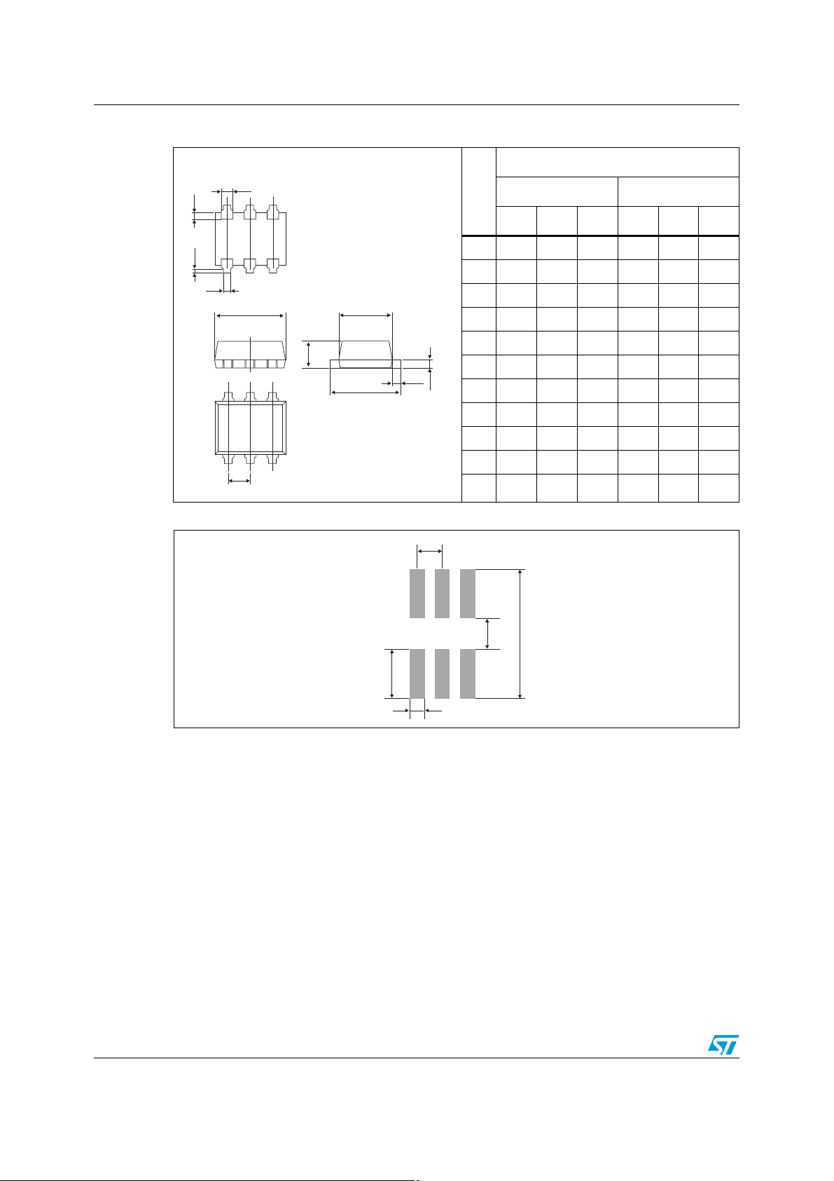
Table 11. SOT323-6L dimensions
Dimensions
A
E
Ref.
A 0.8 1.1 0.031 0.043
e
b
e
A1 0 0.1 0 0.004
D
A2 0.8 1 0.031 0.039
b 0.15 0.3 0.006 0.012
A1
A2
Q1
c
L
HE
c 0.1 0.18 0.004 0.007
D 1.8 2.2 0.071 0.086
E 1.15 1.35 0.045 0.053
e 0.65 Typ. 0.025 Typ.
H 1.8 2.4 0.071 0.094
Q 0.1 0.4 0.004 0.016
Figure 21. SOT323-6L footprint (dimensions in mm)
0.65
1.05
Millimeters Inches
Min. Max. Min. Max.
0.80
2.9
1.05
0.40
Doc ID 12563 Rev 2 11/14
Page 12
Package information BAS70
Table 12. SOT-666 dimensions
Dimensions
b1
L1
L3
Ref.
A 0.45 0.60 0.018 0.024
A3 0.08 0.18 0.003 0.007
b
b 0.17 0.34 0.007 0.013
D
A
E1
b1 0.19 0.27 0.34 0.007 0.011 0.013
D 1.50 1.70 0.059 0.067
L2
E
A3
E 1.50 1.70 0.059 0.067
E1 1.10 1.30 0.043 0.051
e0.50 0.020
L1 0.19 0.007
L2 0.10 0.30 0.004 0.012
e
L3 0.10 0.004
Figure 22. SOT-666 footprint (dimensions in mm)
0.50
Millimeters Inches
Min. Typ. Max. Min. Typ. Max.
0.99
0.30
0.62
2.60
12/14 Doc ID 12563 Rev 2
Page 13
BAS70 Ordering information
4 Ordering information
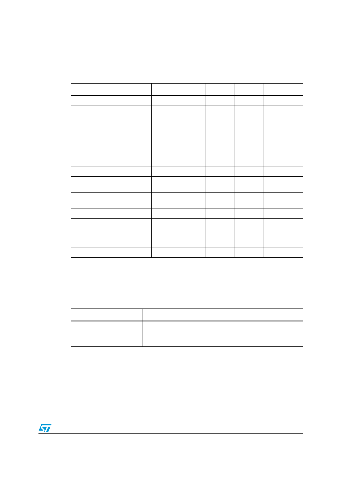
Table 13. Ordering information
Order code Marking Package Weight Base qty Delivery mode
BAS70ZFILM Z70 SOD-123 10 mg 3000 Tape and reel
BAS70FILM D76 SOT-23 Single 10 mg 3000 Tape and reel
BAS70-04FILM D96 SOT-23 Series 10 mg 3000 Tape and reel
BAS70-05FILM D97
BAS70-06FILM D98
BAS70WFILM D28 SOT-323 Single 6 mg 3000 Tape and reel
BAS70-04WFILM D31 SOT-323 Series 6 mg 3000 Tape and reel
SOT-23
Common cathode
SOT-23
Common anode
10 mg 3000 Tape and reel
10 mg 3000 Tape and reel
BAS70-05WFILM D30
BAS70-06WFILM D29
BAS70-08SFILM D33 SOT323-6L 3 Parallel 6 mg 3000 Tape and reel
BAS70JFILM 76 SOD-323 5 mg 3000 Tape and reel
BAS70KFILM 76 SOD-523 1.4 mg 3000 Tape and reel
BAS70-07P6FILM P7 SOT-666 2 Parallel 2.9 mg 3000 Tape and reel
BAS70-09P6FILM Q7 SOT-666 2 Opposite 2.9 mg 3000 Tape and reel
5 Revision history
Table 14. Document revision history
Date Revision Changes
24-Jul-2006 1
12-Oct-2009 2 Updated Table 8 quote “L1” from 0.10 to 0.05.
SOT-323
Common cathode
SOT-323
Common anode
BAS70J / W datasheets merged. ECOPACK statement added. SOD523 and SOT-666 packages added.
6 mg 3000 Tape and reel
6 mg 3000 Tape and reel
Doc ID 12563 Rev 2 13/14
Page 14

BAS70
Please Read Carefully:
Information in this document is provided solely in connection with ST products. STMicroelectronics NV and its subsidiaries (“ST”) reserve the
right to make changes, corrections, modifications or improvements, to this document, and the products and services described herein at any
time, without notice.
All ST products are sold pursuant to ST’s terms and conditions of sale.
Purchasers are solely responsible for the choice, selection and use of the ST products and services described herein, and ST assumes no
liability whatsoever relating to the choice, selection or use of the ST products and services described herein.
No license, express or implied, by estoppel or otherwise, to any intellectual property rights is granted under this document. If any part of this
document refers to any third party products or services it shall not be deemed a license grant by ST for the use of such third party products
or services, or any intellectual property contained therein or considered as a warranty covering the use in any manner whatsoever of such
third party products or services or any intellectual property contained therein.
UNLESS OTHERWISE SET FORTH IN ST’S TERMS AND CONDITIONS OF SALE ST DISCLAIMS ANY EXPRESS OR IMPLIED
WARRANTY WITH RESPECT TO THE USE AND/OR SALE OF ST PRODUCTS INCLUDING WITHOUT LIMITATION IMPLIED
WARRANTIES OF MERCHANTABILITY, FITNESS FOR A PARTICULAR PURPOSE (AND THEIR EQUIVALENTS UNDER THE LAWS
OF ANY JURISDICTION), OR INFRINGEMENT OF ANY PATENT, COPYRIGHT OR OTHER INTELLECTUAL PROPERTY RIGHT.
UNLESS EXPRESSLY APPROVED IN WRITING BY AN AUTHORIZED ST REPRESENTATIVE, ST PRODUCTS ARE NOT
RECOMMENDED, AUTHORIZED OR WARRANTED FOR USE IN MILITARY, AIR CRAFT, SPACE, LIFE SAVING, OR LIFE SUSTAINING
APPLICATIONS, NOR IN PRODUCTS OR SYSTEMS WHERE FAILURE OR MALFUNCTION MAY RESULT IN PERSONAL INJURY,
DEATH, OR SEVERE PROPERTY OR ENVIRONMENTAL DAMAGE. ST PRODUCTS WHICH ARE NOT SPECIFIED AS "AUTOMOTIVE
GRADE" MAY ONLY BE USED IN AUTOMOTIVE APPLICATIONS AT USER’S OWN RISK.
Resale of ST products with provisions different from the statements and/or technical features set forth in this document shall immediately void
any warranty granted by ST for the ST product or service described herein and shall not create or extend in any manner whatsoever, any
liability of ST.
ST and the ST logo are trademarks or registered trademarks of ST in various countries.
Information in this document supersedes and replaces all information previously supplied.
The ST logo is a registered trademark of STMicroelectronics. All other names are the property of their respective owners.
© 2009 STMicroelectronics - All rights reserved
STMicroelectronics group of companies
Australia - Belgium - Brazil - Canada - China - Czech Republic - Finland - France - Germany - Hong Kong - India - Israel - Italy - Japan -
Malaysia - Malta - Morocco - Philippines - Singapore - Spain - Sweden - Switzerland - United Kingdom - United States of America
www.st.com
14/14 Doc ID 12563 Rev 2
 Loading...