

50 / 50+j50 balun transformer for 2.45 GHz ISM band
Features
■ 50 Ω nominal Input / 50+j50 output differential
impedance
■ Low insertion loss
■ Low amplitude imbalance
■ Low phase imbalance
■ Small footprint: BAL-2593D5U < 1.5 mm²
Benefits
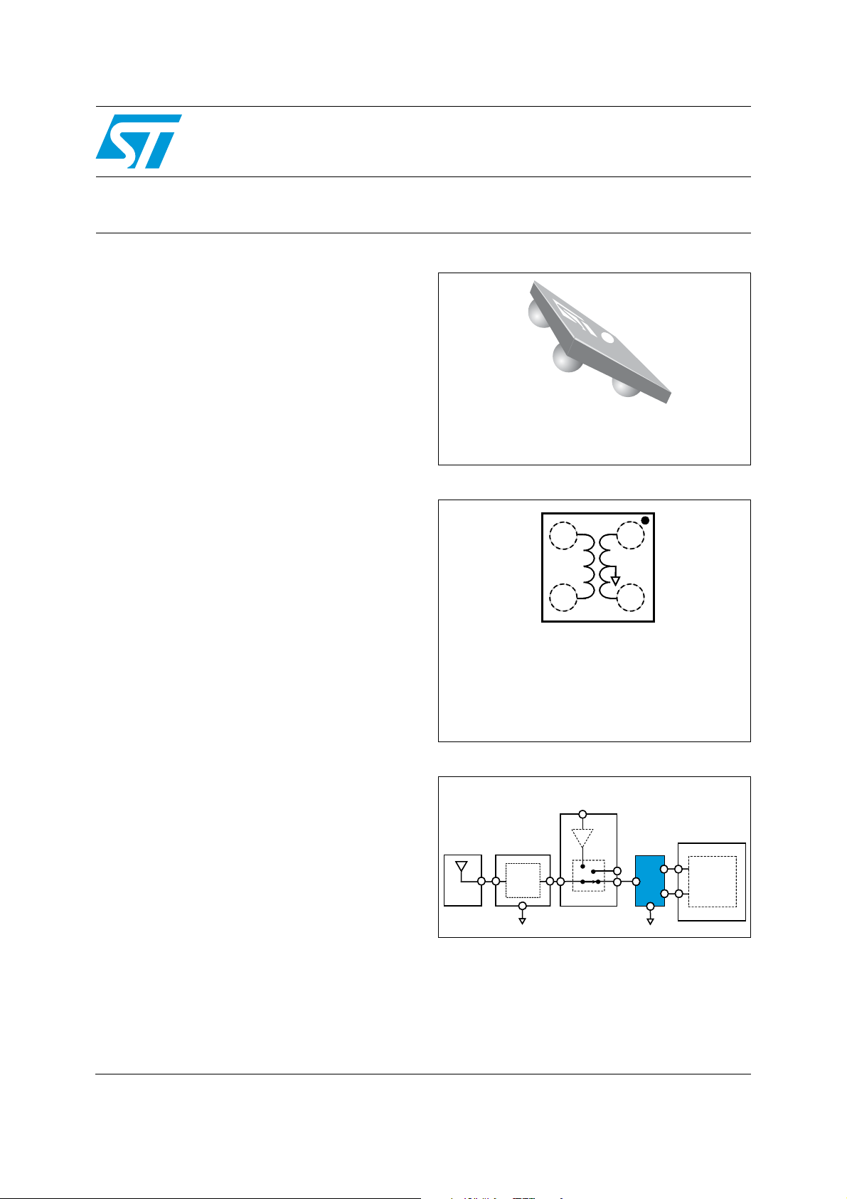
BAL-2593D5U
Flip Chip
4 bumps
■ Very low profile (<700 µm)
■ High RF performances
■ RF components count and area reduction
Application
■ Bluetooth balun for STL2592/2593/2500D
transceiver
■ Portable applications
Description
The BAL-2593D5U is a balun designed to
transform a single ended signal to differential
signals in Bluetooth applications.
This BAL-2593D5U, with less than 1.2 dB
insertion losses in the bandwidth 2400 MHz to
2500 MHz, has been customized for
STLC2592/2593/2500D Bluetooth transceivers
and specific requirements for S
2f0 (4.88 GHz).
The BAL-2593D5U has been designed using
STMicroelectronics IPD (integrated passive
device) technology on non conductive glass
substrate to optimize RF performances.
parameter at
CC22
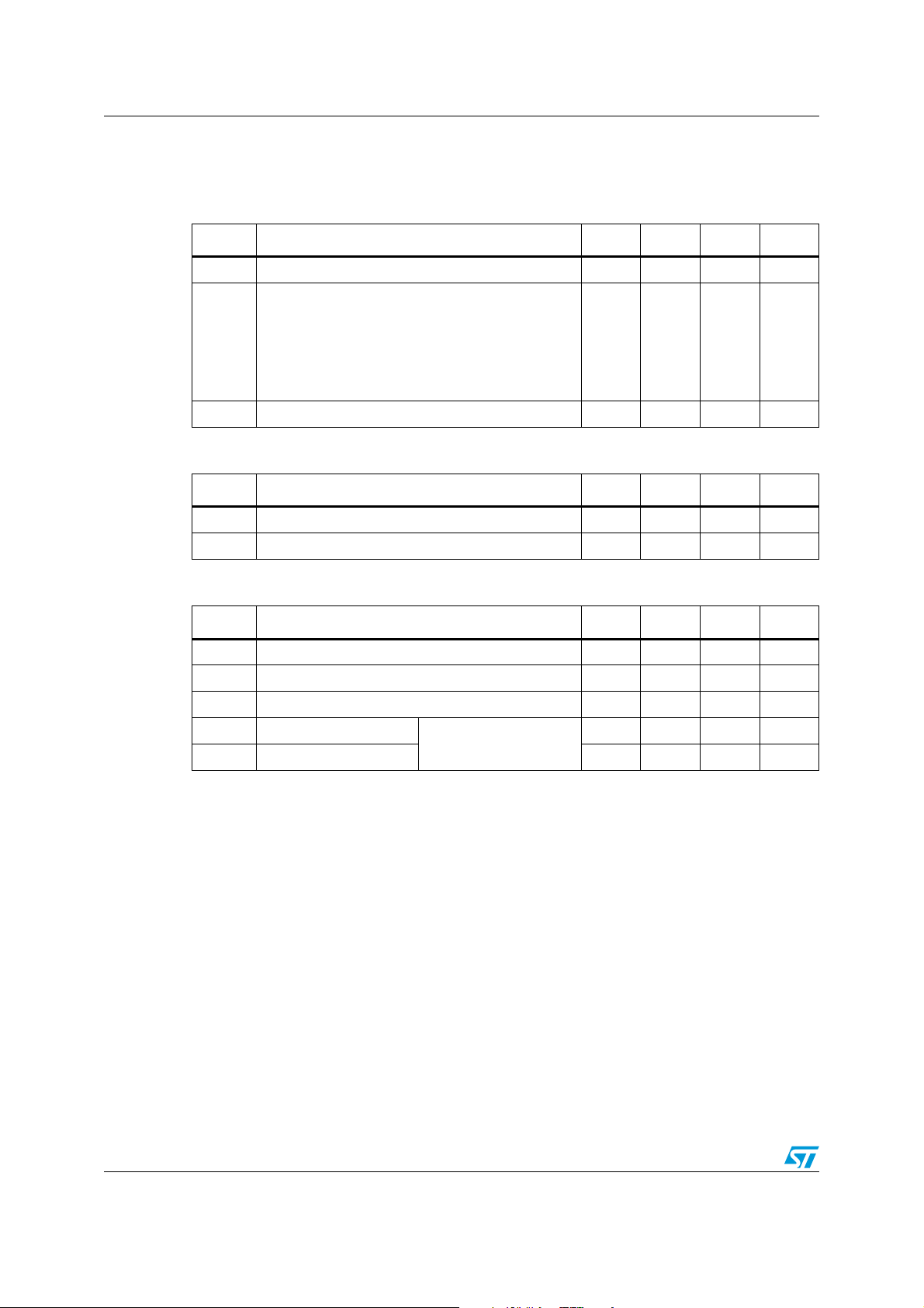
Figure 1. Top view
A1
B1B2
DescriptionBump
RF balanced ouput
Ground
RF balanced ouput
RF input
A1
A2
B1
B2
A2
Name
BALGND
BAL+
SE
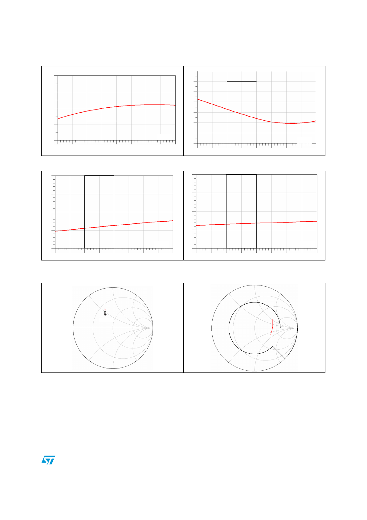
Figure 2. Application schematic
WLAN
PA
+ SP3T
2.4G
Antenna
Band
Pass
Filter
BT
Balun
BT
RFIC
TM: IPAD is a trademark of STMicroelectronics.
October 2009 Doc ID 16008 Rev 1 1/8
www.st.com
8
Electrical characteristics BAL-2593D5U
1 Electrical characteristics
Table 1. Absolute maximum ratings (limiting values)
Symbol Test condition Min. Typ. Max. Unit
P
IN
Input power R
FIN
-10dBm
ESD ratings MIL STD883C
V
(HBM: C = 100 pF, R = 1.5kΩ , air discharge)
ESD ratings machine model
ESD
(MM: C = 200 pF, R = 25 Ω, L = 500 nH)
ESD ratings, charged device model
1000
200
500
--V
(JESD22-C101D)
T
Table 2. Electrical characteristics (T
Operating temperature -30 - +85 °C
OP
= 25 °C) impedances
amb
Symbol Test condition Min. Typ. Max. Unit
Z
Z
Table 3. RF performance (T
Nominal differential output impedance - 50 + j50 - Ω
OUT
Nominal input impedance - 50 - Ω
IN
= 25 °C)
amb
Symbol Test condition Min. Typ. Max. Unit
F Frequency range (bandwidth) 2400 - 2500 MHz
I
Insertion loss in bandwidth - 1.0 1.2 dB
L
R
Return loss in bandwidth 10 17 - dB
L
Φ
A
Phase imbalance
imb
Amplitude imbalance -2 - 2 dB
imb
Measured on EVB with
GND on L1
0620°
2/8 Doc ID 16008 Rev 1
BAL-2593D5U Electrical characteristics
Figure 3. Insertion loss (T
-0.50
-0.75
-1.00
-1.25
-1.50
2.30E9
2.35E9
2.45E92.40E9
Figure 5. Amplitude imbalance (T
2
= 25 °C) Figure 4. Return loss (T
amb
2.55E92.50E9
freq. Hz
= 25 °C) Figure 6. Phase imbalance (T
amb
-8
-10
-12
-14
-16
-18
-20
2.70E92.65E92.60E9
-22
2.30E9
20
2.35E9
2.45E92.40E9
amb
2.55E92.50E9
= 25 °C)
= 25 °C)
amb
freq. Hz
2.70E92.65E92.60E9
1
0
-1
-2
2.30E9
2.35E9
Figure 7. S
freq. Hz
freq. Hz
2.55E92.50E9
= 25 °C),
amb
dd22
2.45E92.40E9
@ f0 (T
freq (2.4000 GHz to 2.500 GHz)
50 + j50
2.70E92.65E92.60E9
15
10
5
0
2.30E9
2.35E9
Figure 8. S
freq. Hz
2.55E92.50E9
= 25 °C),
amb
cc22
2.45E92.40E9
@ 2f0 (T
freq (4.8000 GHz to 5.000 GHz)
2.70E92.65E92.60E9
Doc ID 16008 Rev 1 3/8

Electrical characteristics BAL-2593D5U
Figure 9. Recommend land pattern (used for balun characterization)
35 µm
76 µm
18 µm
540 µm
GND under the die
18 µm
76 µm
35 µm
Figure 10. Example of transceiver application board land pattern
L3
L3
L4
L4
L1
L1
L2
L2
4/8 Doc ID 16008 Rev 1

BAL-2593D5U Package information
2 Package information
● Epoxy meets UL94, V0
● Lead-free package
In order to meet environmental requirements, ST offers these devices in different grades of
ECOPACK
specifications, grade definitions and product status are available at: www.st.com
ECOPACK
Table 4. Package dimensions (values)
®
packages, depending on their level of environmental compliance. ECOPACK®
®
is an ST trademark.
.
Dimensions (mm)
Ref.
Min. Typ. Max.
A 0.61 0.675 0.74
A1 0.21 0.25 0.29
A2 - 0.4 -
b 0.265 0.315 0.365
D 1.21 1.26 1.31
D1 - 0.8 -
E 1.11 1.16 1.21
E1 - 0.7 -
SE - 0.35 -
$-0.025-
Figure 11. Package dimensions (definitions)
b
A2
E
DD
A
D1
Doc ID 16008 Rev 1 5/8
A1
B1B2
SE
E1
$
A2
A1

Package information BAL-2593D5U
Figure 12. Footprint Figure 13. Marking
Copper pad Diameter:
250 µm recommended, 300 µm max
Solder stencil opening: 330 µm
Solder mask opening recommendation:
340 µm min for 315 µm copper pad diameter
Dot, ST logo
ECOPACK®Grade
xx = marking
z = manufacturing location
yww = datecode
(y = year
ww = week)
Figure 14. Flip Chip tape and reel specification
Dot identifying pin A1 location
4.0 ± 0.1
z
z
x
x
x
x
w
w
w
w
y
y
0.20 ± 0.015
1.36 ± 0.05
8.0 ± 0.3
2.0 ± 0.05
z
z
w
w
x
x
w
w
x
y
x
y
Ø 1.50 ± 0.10
z
z
w
w
x
x
w
w
x
y
x
y
xyxwz
w
1.75 ± 0.1
3.5 ± 0.05
1.26 ± 0.05
2.0 ± 0.05
0.73± 0.05
All dimensions in mm
User direction of unreeling
Note: More packing information is available in the applications note:
AN 2348: “Flip Chip: package description and recommendations for use”
6/8 Doc ID 16008 Rev 1

BAL-2593D5U Ordering information
3 Ordering information
Table 5. Ordering information
Order code Marking Package Weight Base qty Delivery mode
BAL-2593D5U RM Flip Chip 1.75 mg 5000 Tape and reel
4 Revision history
Table 6. Document revision history
Date Revision Changes
12-Oct-2009 1 Initial release.
Doc ID 16008 Rev 1 7/8

BAL-2593D5U
Please Read Carefully:
Information in this document is provided solely in connection with ST products. STMicroelectronics NV and its subsidiaries (“ST”) reserve the
right to make changes, corrections, modifications or improvements, to this document, and the products and services described herein at any
time, without notice.
All ST products are sold pursuant to ST’s terms and conditions of sale.
Purchasers are solely responsible for the choice, selection and use of the ST products and services described herein, and ST assumes no
liability whatsoever relating to the choice, selection or use of the ST products and services described herein.
No license, express or implied, by estoppel or otherwise, to any intellectual property rights is granted under this document. If any part of this
document refers to any third party products or services it shall not be deemed a license grant by ST for the use of such third party products
or services, or any intellectual property contained therein or considered as a warranty covering the use in any manner whatsoever of such
third party products or services or any intellectual property contained therein.
UNLESS OTHERWISE SET FORTH IN ST’S TERMS AND CONDITIONS OF SALE ST DISCLAIMS ANY EXPRESS OR IMPLIED
WARRANTY WITH RESPECT TO THE USE AND/OR SALE OF ST PRODUCTS INCLUDING WITHOUT LIMITATION IMPLIED
WARRANTIES OF MERCHANTABILITY, FITNESS FOR A PARTICULAR PURPOSE (AND THEIR EQUIVALENTS UNDER THE LAWS
OF ANY JURISDICTION), OR INFRINGEMENT OF ANY PATENT, COPYRIGHT OR OTHER INTELLECTUAL PROPERTY RIGHT.
UNLESS EXPRESSLY APPROVED IN WRITING BY AN AUTHORIZED ST REPRESENTATIVE, ST PRODUCTS ARE NOT
RECOMMENDED, AUTHORIZED OR WARRANTED FOR USE IN MILITARY, AIR CRAFT, SPACE, LIFE SAVING, OR LIFE SUSTAINING
APPLICATIONS, NOR IN PRODUCTS OR SYSTEMS WHERE FAILURE OR MALFUNCTION MAY RESULT IN PERSONAL INJURY,
DEATH, OR SEVERE PROPERTY OR ENVIRONMENTAL DAMAGE. ST PRODUCTS WHICH ARE NOT SPECIFIED AS "AUTOMOTIVE
GRADE" MAY ONLY BE USED IN AUTOMOTIVE APPLICATIONS AT USER’S OWN RISK.
Resale of ST products with provisions different from the statements and/or technical features set forth in this document shall immediately void
any warranty granted by ST for the ST product or service described herein and shall not create or extend in any manner whatsoever, any
liability of ST.
ST and the ST logo are trademarks or registered trademarks of ST in various countries.
Information in this document supersedes and replaces all information previously supplied.
The ST logo is a registered trademark of STMicroelectronics. All other names are the property of their respective owners.
© 2009 STMicroelectronics - All rights reserved
STMicroelectronics group of companies
Australia - Belgium - Brazil - Canada - China - Czech Republic - Finland - France - Germany - Hong Kong - India - Israel - Italy - Japan -
Malaysia - Malta - Morocco - Philippines - Singapore - Spain - Sweden - Switzerland - United Kingdom - United States of America
www.st.com
8/8 Doc ID 16008 Rev 1
 Loading...