

Page 1

Features
■ Qualified following the AEC-Q100
requirements (temperature Grade 1), see
PPAP for more details.
■ 2 A DC output current
■ Operating input voltage from 4 V to 36 V
■ 3.3 V / (±2 %) reference voltage
■ Output voltage adjustable from 1.235 V to 35 V
■ Low dropout operation: 100 % duty cycle
■ 250 kHz internally fixed frequency
■ Voltage feedforward
■ Zero load current operation
■ Internal current limiting
■ Inhibit for zero current consumption
■ Synchronization
■ Protection against feedback disconnection
■ Thermal shutdown
Applications
■ Dedicated to automotive applications
Figure 1. Typical application
VIN=4V to 35V
VIN=4V to 35V
C1
C1
10uF
10uF
35V
35V
CERAMIC
CERAMIC
C3
C3
220pF
220pF
C4
C4
22nF
22nF
VCC
VCC
COMP
COMP
R3
R3
4k7
4k7
8
8
4
4
VREF
VREF
3.3V
3.3V
6
6
B
A5973D
A5973D
7
7
GND
GND
B5973D
2 A step down switching regulator
for automotive applications
HSOP8 exposed pad
Description
The B5973D is a step down monolithic power
switching regulator with a minimum switch current
limit of 2.25 A so it is able to deliver up to 2 A DC
current to the load depending on the application
conditions. The output voltage can be set from
1.235 V to 35 V. The high current level is also
achieved thanks to an SO8 package with exposed
frame, that allows to reduce the R
approximately 40 °C/W. The device uses an
internal P-channel DMOS transistor (with a typical
R
of 250 mΩ) as switching element to
DSon
minimize the size of the external components. An
internal oscillator fixes the switching frequency at
250 kHz. Having a minimum input voltage of 4V
only, it is particularly suitable for 5 V bus. Pulse by
pulse current limit with the internal frequency
modulation offers an effective constant current
short circuit protection. Pulse by pulse current
limit with the internal frequency modulation offers
an effective constant current short circuit
protection.
L1 15uH
L1 15uH
OUT
OUT
1
1
SYNCH
SYNCH
2
INH
INH
2
FB
FB
5
5
3
3
D1
D1
STPS340U
STPS340U
R1
R1
5k6
5k6
R2
R2
3k3
3k3
th(JA)
down to
Vout=3.3V
Vout=3.3V
C2
C2
330uF
330uF
6.3V
6.3V
August 2008 Rev 3 1/11
www.st.com
1
Page 2

B5973D Contents
Contents
1 Pin settings . . . . . . . . . . . . . . . . . . . . . . . . . . . . . . . . . . . . . . . . . . . . . . . . 2
1.1 Pin connection . . . . . . . . . . . . . . . . . . . . . . . . . . . . . . . . . . . . . . . . . . . . . . 2
1.2 Pin description . . . . . . . . . . . . . . . . . . . . . . . . . . . . . . . . . . . . . . . . . . . . . . 2
2 Electrical data . . . . . . . . . . . . . . . . . . . . . . . . . . . . . . . . . . . . . . . . . . . . . . 3
2.1 Maximum ratings . . . . . . . . . . . . . . . . . . . . . . . . . . . . . . . . . . . . . . . . . . . . 3
2.2 Thermal data . . . . . . . . . . . . . . . . . . . . . . . . . . . . . . . . . . . . . . . . . . . . . . . 3
3 Electrical characteristics . . . . . . . . . . . . . . . . . . . . . . . . . . . . . . . . . . . . . 4
4 Typical characteristics . . . . . . . . . . . . . . . . . . . . . . . . . . . . . . . . . . . . . . . 6
5 Package mechanical data . . . . . . . . . . . . . . . . . . . . . . . . . . . . . . . . . . . . . 8
6 Revision history . . . . . . . . . . . . . . . . . . . . . . . . . . . . . . . . . . . . . . . . . . . 10
1/11
Page 3
B5973D
1 Pin settings
1.1 Pin connection
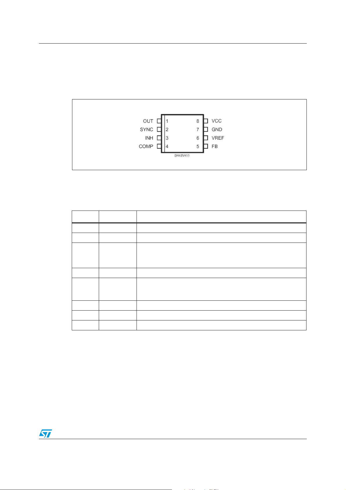
Figure 2. Pin connection (top view)
1.2 Pin description
Table 1. Pin description
N° Pin Description
1 OUT Regulator output.
2 SYNCH Master/slave synchronization.
A logical signal (active high) disables the device. If INH not used the pin
3INH
4 COMP E/A output for frequency compensation.
5FB
6 VREF 3.3 V V
7 GND Ground.
8 VCC Unregulated DC input voltage.
must be grounded. When it is open an internal pull-up disable the
device.
Feedback input. Connecting directly to this pin results in an output
voltage of 1.23 V. An extenal resistive divider is required for higher
output voltages.
REF. No cap is requested for stability.
2/11
Page 4
Electrical data B5973D
2 Electrical data
2.1 Maximum ratings
Table 2. Absolute maximum ratings
Symbol Parameter Value Unit
V
8
V
1
I
1
V
, V
4
V
3
V
2
P
TOT
T
j
T
STG
Input voltage 40 V
OUT pin DC voltage
OUT pin peak voltage at Δt = 0.1μs
Maximum output current int. limit.
Analog pins 4 V
5
INH -0.3 to V
SYNCH -0.3 to 4 V
Power dissipation at TA ≤ 70 °C 2.25 W
Operating junction temperature range -40 to 150 °C
Storage temperature range -55 to 150 °C
2.2 Thermal data
Table 3. Thermal data
Symbol Parameter SO8 Unit
R
thJA Maximum thermal resistance junction-ambient 40
1. Package mounted on board
-1 to 40
-5 to 40
(1)
CC
V
V
V
°C/W
3/11
Page 5

B5973D
3 Electrical characteristics
Table 4. Electrical characteristics
(T
= -40 °C to 125 °C, V
J
Symbol Parameter Test condition Min Typ Max Unit
= 12 V, unless otherwise specified)
CC
V
R
DS(on)
f
CC
I
L
SW
Operating input
voltage range
MOSFET on
resistance
Maximum limiting
current
(1)
Switching frequency 212 250 280 kHz
= 1.235 V; I0 = 2 A 4 36 V
V
0
V
CC
= 5 V, TJ = 25 °C 2.5 3 3.5
V
CC
Duty cycle 0 100 %
Dynamic characteristics (see test circuit).
V
Voltage feedback
5
η Efficiency V
4.4 V < V
20 mA < I0 < 2 A
= 5 V, V
0
DC characteristics
I
qop
I
I
qst-by
Total operating
quiescent current
Quiescent current Duty cycle = 0; V
q
V
Total stand-by
quiescent current
V
V
> 2.2 V 50 100 μA
inh
CC
> 2.2 V
inh
Inhibit
Device ON 0.8 V
INH threshold voltage
Device OFF 2.2 V
0.250 0.5 Ω
= 5 V 2.25 3 3.5
< 36 V,
CC
= 12 V 90 %
CC
1.198 1.235 1.272 V
35mA
= 1.5 V 2.5 mA
FB
= 36 V;
80 150 μA
A
Error amplifier
V
OH
V
Io source
I
o sink Sink output current
I
High level output
voltage
Low level output
OL
voltage
Source output current
b Source bias current 2.5 4 μA
DC open loop gain R
V
= 1 V 3.5 V
FB
= 1.5 V 0.4 V
V
FB
V
= 1.9 V; VFB = 1 V
COMP
V
= 1.9 V; V
COMP
L = ∞ 50 65 dB
FB
= 1.5 V
190 300 μA
11.5 mA
4/11
Page 6

Electrical characteristics B5973D
Table 4. Electrical characteristics
(T
= -40 °C to 125 °C, V
J
Symbol Parameter Test condition Min Typ Max Unit
gm Transconductance
Synch function
= 12 V, unless otherwise specified)
CC
I
= -0.1 mA to 0.1 mA;
COMP
V
= 1.9 V
COMP
2.3 mS
High input voltage
Low input voltage
Slave synch current
Master output
amplitude
Output pulse width
Reference section
Reference voltage
Line regulation
Load regulation
Short circuit current 5 18 35 mA
1. With TJ = 85 °C, I
2. Guarantee by design
lim_min
= 4.4 to 36 V;
V
CC
= 4.4 to 36 V;
V
CC
synch
(2)
= 1.65 V
V
= 0.74 V
synch
V
= 2.33 V
synch
= 3 mA
I
source
no load, V
I
= 0 to 5 mA
REF
V
= 4.4 V to 36 V
CC
I
= 0 mA
REF
= 4.4 V to 36 V
V
CC
I
= 0 mA
REF
= 2.5 A, assured by design, characterization and statistical correlation.
2.5 V
0.11
0.21
2.75 3 V
0.20 0.35 μs
3.2 3.3 3.399 V
510mV
815mV
REF
0.74 V
0.25
0.45
mA
V
5/11
Page 7

B5973D
4 Typical characteristics
Figure 3. Line regulation Figure 4. Shutdown current vs
junction temperature
Figure 5. Output voltage vs junction
temperature
Figure 7. Quiescent current vs
junction temperature
Figure 6. Switching frequency vs
junction temperature
6/11
Page 8

Typical characteristics B5973D
Figure 8. Junction temperature vs
Figure 10. Efficiency vs output current Figure 11. Efficiency vs output current
output current
Figure 9. Junction temperature vs
output current
7/11
Page 9

B5973D
5 Package mechanical data
In order to meet environmental requirements, ST offers these devices in ECOPACK®
packages. These packages have a lead-free second level interconnect. The category of
second level interconnect is marked on the package and on the inner box label, in
compliance with JEDEC Standard JESD97. The maximum ratings related to soldering
conditions are also marked on the inner box label. ECOPACK is an ST trademark.
ECOPACK specifications are available at: www.st.com
8/11
Page 10

Package mechanical data B5973D
Table 5. HSOP8 mechanical data
mm inch
Dim
Min Typ Max Min Typ Max
A 1.70 0.0669
A1 0.00 0.10 0.00 0.0039
A2 1.25 0.0492
b 0.31 0.51 0.0122 0.0201
c 0.17 0.25 0.0067 0.0098
D 4.80 4.90 5.00 0.1890 0.1929 0.1969
D1 3 3.1 3.2 0.118 0.122 0.126
E 5.80 6.00 6.20 0.2283 0.2441
E1 3.80 3.90 4.00 0.1496 0.1575
E2 2.31 2.41 2.51 0.091 0.095 0.099
e1.27
h 0.25 0.50 0.0098 0.0197
L 0.40 1.27 0.0157 0.0500
k0° (min), 8° (max)
ccc 0.10 0.0039
Figure 12. Package dimensions
9/11
Page 11

B5973D
6 Revision history
Table 6. Document revision history
Date Revision Changes
07-Nov-2007 1 Initial release
14-Jan-2008 2 Updated Table 5 on page 9
27-Aug-2008 3 Updated: Coverpage and Table 4 on page 4
10/11
Page 12

B5973D
Please Read Carefully:
Information in this document is provided solely in connection with ST products. STMicroelectronics NV and its subsidiaries (“ST”) reserve the
right to make changes, corrections, modifications or improvements, to this document, and the products and services described herein at any
time, without notice.
All ST products are sold pursuant to ST’s terms and conditions of sale.
Purchasers are solely responsible for the choice, selection and use of the ST products and services described herein, and ST assumes no
liability whatsoever relating to the choice, selection or use of the ST products and services described herein.
No license, express or implied, by estoppel or otherwise, to any intellectual property rights is granted under this document. If any part of this
document refers to any third party products or services it shall not be deemed a license grant by ST for the use of such third party products
or services, or any intellectual property contained therein or considered as a warranty covering the use in any manner whatsoever of such
third party products or services or any intellectual property contained therein.
UNLESS OTHERWISE SET FORTH IN ST’S TERMS AND CONDITIONS OF SALE ST DISCLAIMS ANY EXPRESS OR IMPLIED
WARRANTY WITH RESPECT TO THE USE AND/OR SALE OF ST PRODUCTS INCLUDING WITHOUT LIMITATION IMPLIED
WARRANTIES OF MERCHANTABILITY, FITNESS FOR A PARTICULAR PURPOSE (AND THEIR EQUIVALENTS UNDER THE LAWS
OF ANY JURISDICTION), OR INFRINGEMENT OF ANY PATENT, COPYRIGHT OR OTHER INTELLECTUAL PROPERTY RIGHT.
UNLESS EXPRESSLY APPROVED IN WRITING BY AN AUTHORIZED ST REPRESENTATIVE, ST PRODUCTS ARE NOT
RECOMMENDED, AUTHORIZED OR WARRANTED FOR USE IN MILITARY, AIR CRAFT, SPACE, LIFE SAVING, OR LIFE SUSTAINING
APPLICATIONS, NOR IN PRODUCTS OR SYSTEMS WHERE FAILURE OR MALFUNCTION MAY RESULT IN PERSONAL INJURY,
DEATH, OR SEVERE PROPERTY OR ENVIRONMENTAL DAMAGE. ST PRODUCTS WHICH ARE NOT SPECIFIED AS "AUTOMOTIVE
GRADE" MAY ONLY BE USED IN AUTOMOTIVE APPLICATIONS AT USER’S OWN RISK.
Resale of ST products with provisions different from the statements and/or technical features set forth in this document shall immediately void
any warranty granted by ST for the ST product or service described herein and shall not create or extend in any manner whatsoever, any
liability of ST.
ST and the ST logo are trademarks or registered trademarks of ST in various countries.
Information in this document supersedes and replaces all information previously supplied.
The ST logo is a registered trademark of STMicroelectronics. All other names are the property of their respective owners.
© 2008 STMicroelectronics - All rights reserved
STMicroelectronics group of companies
Australia - Belgium - Brazil - Canada - China - Czech Republic - Finland - France - Germany - Hong Kong - India - Israel - Italy - Japan -
Malaysia - Malta - Morocco - Singapore - Spain - Sweden - Switzerland - United Kingdom - United States of America
www.st.com
11/11
 Loading...